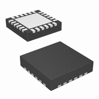
SI4313-B1-FM Silicon Laboratories Inc, SI4313-B1-FM Datasheet - Page 18

SI4313-B1-FM
Manufacturer Part Number
SI4313-B1-FM
Description
IC RX FSK 315-915MHZ 20VQFN
Manufacturer
Silicon Laboratories Inc
Series
EZRadio®r
Type
ISM Receiverr
Specifications of SI4313-B1-FM
Package / Case
20-VQFN
Mfg Application Notes
Si4313 Register Desc AppNote
Frequency
315MHz, 434MHz, 868MHz, 915MHz
Sensitivity
-118dBm
Data Rate - Maximum
128kbps
Modulation Or Protocol
FSK, GFSK, OOK
Applications
Data Logging, Health Monitors, Remote Control, Weather Station
Data Interface
PCB, Surface Mount
Antenna Connector
PCB, Surface Mount
Voltage - Supply
1.8 V ~ 3.6 V
Operating Temperature
-40°C ~ 85°C
Operating Frequency
315 MHz to 915 MHz
Operating Supply Voltage
1.8 V to 3.6 V
Maximum Operating Temperature
+ 85 C
Minimum Operating Temperature
- 40 C
Mounting Style
SMD/SMT
Supply Current
100 nA
Lead Free Status / RoHS Status
Lead free / RoHS Compliant
Features
-
Memory Size
-
Current - Receiving
-
Lead Free Status / Rohs Status
Lead free / RoHS Compliant
Other names
336-1980-5
Available stocks
Company
Part Number
Manufacturer
Quantity
Price
Company:
Part Number:
SI4313-B1-FMR
Manufacturer:
TI
Quantity:
10 000
Part Number:
SI4313-B1-FMR
Manufacturer:
SILICON LABS/芯科
Quantity:
20 000
Si4313-B1
The SPI interface contains a burst read/write mode, which allows for reading/writing sequential registers without
having to resend the SPI address. When the nSEL bit is held low while continuing to send SCLK pulses, the SPI
interface will automatically increment the ADDR and read from/write to the next address. An example burst write
transaction is shown in Figure 4, and a burst read is shown in Figure 5. As long as nSEL is held low, input data will
be latched into the Si4313 every eight SCLK cycles.
18
SDO
SCLK
nSEL
SDI
SDO
SCLK
nSEL
SCLK
nSEL
SDI
SDI
First Bit
First Bit
First Bit
RW
RW
=1
=0
RW
A6
=0
A6
A5
A5
A6
A4
A4
A5
A3
A3
A4
A2
A2
Figure 4. SPI timing—Burst Write Mode
Figure 5. SPI timing—Burst Read Mode
Figure 3. SPI Timing—READ Mode
A3
A1
A1
First Bit
A0
A0
A2
D7
=X
D7
D7
=X
A1
D6 D5 D4 D3
D6
=X
D6
=X
First Bit
A0
D5
=X
D5
=X
Rev. 1.0
D4
=X
D4
=X
D7
D7
=X
D3
=X
D3
=X
D6 D5 D4 D3
D6
=X
D2
=X
D2
=X
D2 D1 D0
Last Bit
D1
=X
D5
=X
D1
=X
D0
=X
D0
=X
D4
=X
D7
=X
D7 D6 D5 D4 D3
D3
=X
D6
=X
D2 D1 D0
D2
=X
D5
=X
D4
=X
D1
=X
D3
=X
Last Bit
D0
=X
Last Bit
D2
=X
D2 D1 D0
D1
=X
Last Bit
D0
=X


