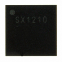
SX1210I084T Semtech, SX1210I084T Datasheet - Page 15

SX1210I084T
Manufacturer Part Number
SX1210I084T
Description
IC SINGLE-CHIP RECEIVER 32-TQFN
Manufacturer
Semtech
Datasheet
1.SX1210I084T.pdf
(73 pages)
Specifications of SX1210I084T
Frequency
863MHz ~ 960MHz
Sensitivity
-113dBm
Data Rate - Maximum
200 kbps
Modulation Or Protocol
FSK, OOK
Applications
Alarm Systems, Communication Systems
Current - Receiving
3mA
Data Interface
PCB, Surface Mount
Antenna Connector
PCB, Surface Mount
Voltage - Supply
2.1 V ~ 3.6 V
Operating Temperature
-40°C ~ 85°C
Package / Case
32-TQFN
Lead Free Status / RoHS Status
Lead free / RoHS Compliant
Features
-
Memory Size
-
The integrated VCO requires only two external tank circuit inductors. As the input is differential, the two inductors
should have the same nominal value. The performance of these components is important for both the phase noise
and the power consumption of the PLL. It is recommended that a pair of high Q factor inductors is selected. These
should be mounted orthogonally to other inductors (in particular the LNA biasing inductor) to reduce spurious
coupling between the LNA input and VCO.
For best performance wound type inductors, with tight tolerance, should be used as described in section 7.5.3.
To guarantee the optimum operation of the VCO over the SX1210’s frequency and temperature ranges, the
following settings should be programmed into the SX1210:
Table 9: MCParam_Freq_band Setting
To ensure that the frequency band of operation may be accurately addressed by the R, P and S dividers of the
synthesizer, it is necessary to ensure that the VCO is correctly centered. Note that for the reference design (see
section 7.5) no centering is necessary. However, any deviation from the reference design may require the
optimization procedure, outlined below, to be implemented. This procedure is simplified thanks to the built-in VCO
trimming feature which is controlled over the SPI interface. This tuning does not require any RF test equipment,
and can be achieved by simply measuring Vtune, the voltage between pins 6 (LFM) and 7 (LFP).
The VCO is centered if the voltage is within the range:
If this inequality is not satisfied then adjust the MCParam_VCO_trim bits from 00 whilst monitoring Vtune. This
allows the VCO voltage to be trimmed in + 60 mV increments. Should the desired voltage range be inaccessible,
the voltage may be adjusted further by changing the tank circuit inductance value. Note that an increase in
inductance will result in an increase Vtune.
Note for mass production: The VCO capacitance is piece to piece dependant. As such, the optimization proposed
above should be verified on several prototypes, to ensure that the population is centered on 100 mV.
To adequately reject spurious components arising from the comparison frequency Fcomp, an external 2
loop filter is employed.
Rev 2– Sept 8
ADVANCED COMMUNICATIONS & SENSING
Target channel
Freq_band
(MHz)
3.2.5. Voltage Controlled Oscillator
3.2.6. PLL Loop Filter
th
, 2008
3.2.5.1. SW Settings of the VCO
3.2.5.2. Trimming the VCO Tank by Hardware and Software
863-
870
10
902-
915
00
915-
928
01
50 ≤
950-
960
10
Vtune
Page 15 of 73
(
mV
)
≤
150
mV
www.semtech.com
SX1210
nd
order


