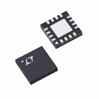
LT5520EUF Linear Technology, LT5520EUF Datasheet - Page 6

LT5520EUF
Manufacturer Part Number
LT5520EUF
Description
IC MIXER UPCONV 1.3-2.3GHZ 16QFN
Manufacturer
Linear Technology
Series
LT5520r
Datasheet
1.LT5520EUF.pdf
(12 pages)
Specifications of LT5520EUF
Rf Type
General Purpose
Frequency
1.3GHz ~ 2.3GHz
Number Of Mixers
1
Gain
-1dB
Noise Figure
15dB
Secondary Attributes
Up Converter
Current - Supply
70mA
Voltage - Supply
4.5 V ~ 5.25 V
Package / Case
16-WQFN Exposed Pad
Operating Temperature (min)
-40C
Operating Temperature (max)
85C
Operating Temperature Classification
Industrial
Lead Free Status / RoHS Status
Contains lead / RoHS non-compliant
Available stocks
Company
Part Number
Manufacturer
Quantity
Price
Company:
Part Number:
LT5520EUF
Manufacturer:
LT
Quantity:
10 000
Part Number:
LT5520EUF#PBF
Manufacturer:
LINEAR/凌特
Quantity:
20 000
Part Number:
LT5520EUF#TRPBF
Manufacturer:
LINEAR/凌特
Quantity:
20 000
LT5520
APPLICATIO S I FOR ATIO
The LT5520 consists of a double-balanced mixer, a high-
performance LO buffer, and bias/enable circuits. The RF
and LO ports may be driven differentially; however, they
are intended to be used in single-ended mode by connect-
ing one input of each pair to ground. The IF input ports
must be DC-isolated from the source and driven differen-
tially. The IF input should be impedance-matched for the
desired input frequency. The LO input has an internal
broadband 50 match with return loss better than 10dB
at frequencies up to 3000MHz. The RF output band ranges
from 1300MHz to 2300MHz, with an internal RF trans-
former providing a 50
band. Low side or high side LO injection can be used.
IF Input Port
The IF inputs are connected to the emitters of the double-
balanced mixer transistors, as shown in Figure 3. These
pins are internally biased and an external resistor must be
connected from each IF pin to ground to set the current
through the mixer core. The circuit has been optimized to
work with 100 resistors, which will result in approxi-
mately 18mA of DC current per side. For best LO leakage
performance, the resistors should be well matched; thus
6
TEST CIRCUIT
0.062"
140MHz
0.018"
0.018"
IF
IN
1
2
3
1760MHz
ER = 4.4
T1
LO
IN
5
4
C1
C2
RF
GND
DC
GND
C3
R1
R2
U
V
EN
CC
1
2
3
4
GND
GND
IF
IF
GND
EN
C5
+
–
16
5
U
impedance match across the
V
LO
CC1
15
6
–
LT5520
V
LO
CC2
C4
W
14
7
+
V
GND
GND
GND
RF
CC3
RF
13
+
–
8
Figure 2. Test Schematic for the LT5520
L1
12
11
10
9
U
5520 TC01
RF
1900MHz
OUT
REF DES
C1, C2
C3
C4
C5
L1
R1, R2
T1
resistors with 0.1%, tolerance are recommended. If LO
leakage is not a concern, then lesser tolerance resistors
can be used. The symmetry of the layout is also important
for achieving optimum LO isolation.
The capacitors shown in Figure 3, C1 and C2, serve two
purposes. They provide DC isolation between the IF
IF
cause unpredictable variations in LO leakage. They also
improve the impedance match by canceling excess induc-
tance in the package and transformer. The input capacitor
value required to realize an impedance match at desired
frequency, f, can be estimated as follows:
where; f is in units of Hz, L
are in farad. L
LT5520, and is approximately 1.67nH. L
combined inductances of differential external compo-
nents and transmission lines. For the evaluation board
shown in Figure 10, L
the above formula gives C1 = C2 = 220pF.
–
C
ports, thus preventing DC interactions that could
1
C
100 , 0.1%
2
1000pF
VALUE
220pF
39nH
15pF
1 F
4:1
2 ( ) (
IN
is the differential input inductance of the
f L
2
SM-22
EXT
0402
0402
0402
0603
0402
0603
SIZE
IN
1
= 4.21nH. Thus, for f = 140MHz,
IN
L
EXT
and L
PART NUMBER
AVX 04023C221KAT2A
AVX 04023A150KAT2A
AVX 04023A102KAT2A
Taiyo Yuden LMK107BJ105MA
Toko LL1005-FH39NJ
IRC PFC-W0603R-03-10R1-B
M/A-COM ETC4-1-2
)
EXT
are in H, and C1, C2
EXT
represents the
+
and
5520f


