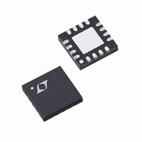
LT5520EUF Linear Technology, LT5520EUF Datasheet - Page 5

LT5520EUF
Manufacturer Part Number
LT5520EUF
Description
IC MIXER UPCONV 1.3-2.3GHZ 16QFN
Manufacturer
Linear Technology
Series
LT5520r
Datasheet
1.LT5520EUF.pdf
(12 pages)
Specifications of LT5520EUF
Rf Type
General Purpose
Frequency
1.3GHz ~ 2.3GHz
Number Of Mixers
1
Gain
-1dB
Noise Figure
15dB
Secondary Attributes
Up Converter
Current - Supply
70mA
Voltage - Supply
4.5 V ~ 5.25 V
Package / Case
16-WQFN Exposed Pad
Operating Temperature (min)
-40C
Operating Temperature (max)
85C
Operating Temperature Classification
Industrial
Lead Free Status / RoHS Status
Contains lead / RoHS non-compliant
Available stocks
Company
Part Number
Manufacturer
Quantity
Price
Company:
Part Number:
LT5520EUF
Manufacturer:
LT
Quantity:
10 000
Part Number:
LT5520EUF#PBF
Manufacturer:
LINEAR/凌特
Quantity:
20 000
Part Number:
LT5520EUF#TRPBF
Manufacturer:
LINEAR/凌特
Quantity:
20 000
PI FU CTIO S
BLOCK DIAGRA
GND (Pins 1, 4, 9, 12, 13, 16): Internal Grounds. These
pins are used to improve isolation and are not intended as
DC or RF grounds for the IC. Connect these pins to low
impedance grounds for best performance.
IF
ential signal must be applied to these pins through DC
blocking capacitors. The pins must be connected to ground
with 100 resistors (the grounds must each be capable of
sinking about 18mA). For best LO leakage performance,
these pins should be DC isolated from each other. An
impedance transformation is required to match the IF
input to the desired source impedance (typically 50 or
75 ).
EN (Pin 5): Enable Pin. When the applied voltage is greater
than 3V, the IC is enabled. When the applied voltage is less
than 0.5V, the IC is disabled and the DC current drops to
about 1 A.
V
Typical current consumption is about 2mA. This pin
should be externally connected to V
ate RF bypass capacitors.
V
Typical current consumption is about 22mA. This pin
should have appropriate RF bypass capacitors as shown
CC1
CC2
+
U
, IF
(Pin 7): Power Supply Pin for the LO Buffer Circuits.
(Pin 6): Power Supply Pin for the Bias Circuits.
–
(Pins 2, 3): Differential IF Signal Inputs. A differ-
U
U
W
GND
GND
LO
LO
+
–
CC
13
14
15
16
and have appropri-
85
5pF
5pF
BACKSIDE
GROUND
V
CC2
17
HIGH SPEED
7
LO BUFFER
GND
GND
12
1
in Figure 2. The 1000pF capacitor should be located as
close to the pins as possible.
V
Typical current consumption is about 36mA. This pin
should be externally connected to V
tor. A 39nH inductor is used in Figure 2, though the value
is not critical.
RF
may be DC connected to a low impedance ground to realize
a 50 single-ended output. No external matching compo-
nents are required. A DC voltage should not be applied
across these pins, as they are internally connected through
a transformer winding.
LO
puts. The LT5520 works well with a single-ended source
driving the LO
impedance ground. No external matching components are
required. An internal resistor is connected across these
pins; therefore, a DC voltage should not be applied across
the inputs.
GROUND (Pin 17, Exposed Pad): DC and RF ground
return for the entire IC. This must be soldered to the
printed circuit board low impedance ground plane.
RF
IF
11
2
CC3
+
+
+
–
, LO
, RF
(Pin 8): Power Supply Pin for the Internal Mixer.
RF
IF
10
3
–
–
DOUBLE-
BALANCED
MIXER
+
–
(Pins 10, 11): Differential RF Outputs. One pin
10pF
(Pins 14, 15): Differential Local Oscillator In-
GND
GND
9
4
BIAS
+
5520 BD
pin and the LO
8
6
5
V
V
EN
CC3
CC1
–
pin connected to a low
CC
through an induc-
LT5520
5
5520f


