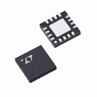
LT5520EUF Linear Technology, LT5520EUF Datasheet - Page 3

LT5520EUF
Manufacturer Part Number
LT5520EUF
Description
IC MIXER UPCONV 1.3-2.3GHZ 16QFN
Manufacturer
Linear Technology
Series
LT5520r
Datasheet
1.LT5520EUF.pdf
(12 pages)
Specifications of LT5520EUF
Rf Type
General Purpose
Frequency
1.3GHz ~ 2.3GHz
Number Of Mixers
1
Gain
-1dB
Noise Figure
15dB
Secondary Attributes
Up Converter
Current - Supply
70mA
Voltage - Supply
4.5 V ~ 5.25 V
Package / Case
16-WQFN Exposed Pad
Operating Temperature (min)
-40C
Operating Temperature (max)
85C
Operating Temperature Classification
Industrial
Lead Free Status / RoHS Status
Contains lead / RoHS non-compliant
Available stocks
Company
Part Number
Manufacturer
Quantity
Price
Company:
Part Number:
LT5520EUF
Manufacturer:
LT
Quantity:
10 000
Part Number:
LT5520EUF#PBF
Manufacturer:
LINEAR/凌特
Quantity:
20 000
Part Number:
LT5520EUF#TRPBF
Manufacturer:
LINEAR/凌特
Quantity:
20 000
DC ELECTRICAL CHARACTERISTICS
(Test Circuit Shown in Figure 2) V
PARAMETER
Enable = High (On)
Enable = Low (Off)
Power Supply Requirements (V
Supply Voltage
Supply Current
Shutdown Current
Note 1: Absolute Maximum Ratings are those values beyond which the life
of a device may be impaired.
Note 2: External components on the final test circuit are optimized for
operation at f
V
unless otherwise noted. For 2-tone inputs: 2nd IF input = 141MHz at –10dBm. (Test Circuit Shown in Figure 2.)
TYPICAL PERFOR A CE CHARACTERISTICS
CC
–4
18
16
14
12
10
–2
= 5V
8
6
4
2
0
1300
Conversion Gain and SSB Noise
Figure vs RF Output Frequency
SSB NF
GAIN
HIGH SIDE LO
DC
1500
, EN = High, T
RF
RF OUTPUT FREQUENCY (MHz)
LOW SIDE AND HIGH SIDE LO
LOW SIDE LO
= 1900MHz, f
1700
66
64
62
60
58
56
54
52
50
1900
4.0
Supply Current
vs Supply Voltage
A
LO
= 25 C, IF input = 140MHz at –10dBm, LO input = 1.76GHz at –5dBm, RF output measured at 1900MHz,
2100
= 1.76GHz and f
CC
4.25
)
T
W
A
SUPPLY VOLTAGE (V)
2300
CC
= 85 C
4.5
5520 • GO3
= 5V
T
A
2500
U
= 25 C
4.75
DC
IF
T
, EN = High , T
A
= 140MHz.
= –40 C
5.0
32
30
28
26
24
22
20
18
16
14
12
1300
IIP3 and IIP2
vs RF Output Frequency
5.25
IIP3
HIGH SIDE LO
5520 • GO1
1500
LOW SIDE LO
CONDITIONS
V
EN = Low
RF OUTPUT FREQUENCY (MHz)
CC
5.5
A
= 25 C (Note 3), unless otherwise noted.
= 5V
1700
DC
LOW SIDE LO
1900
HIGH SIDE LO
Note 3: Specifications over the –40 C to 85 C temperature range are
assured by design, characterization and correlation with statistical process
controls.
Note 4: Turn-On and Turn-Off times are based on the rise and fall times of
the RF output envelope from full power to –40dBm with an IF input power
of –10dBm.
2100
2300
1.0
0.9
0.8
0.7
0.6
0.5
0.4
0.3
0.2
0.1
5520 • GO4
0
IIP2
4.0
Shutdown Current
vs Supply Voltage
(Test Circuit Shown in Figure 2)
2500
55
50
45
40
35
30
25
20
15
10
5
4.25
T
A
= 85 C
SUPPLY VOLTAGE (V)
4.5
–50
–60
–10
–20
–30
–40
4.75
1300
T
A
LO-RF Leakage
vs RF Output Frequency
= 25 C
HIGH SIDE LO
MIN
LOW SIDE LO
3
5.0
1500
RF OUTPUT FREQUENCY (MHz)
T
A
4.5 to 5.25
5.25
= –40 C
1700
5520 • GO2
TYP
60
1
5.5
1900
LT5520
MAX
2100
100
0.5
70
2300
5520 • GO5
UNITS
3
5520f
V
V
V
2500
mA
DC
DC
DC
A


