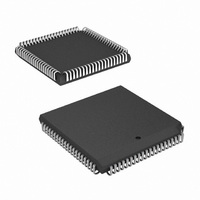
HSP50210JI-52Z Intersil, HSP50210JI-52Z Datasheet - Page 23

HSP50210JI-52Z
Manufacturer Part Number
HSP50210JI-52Z
Description
IC DEMODULATOR COSTAS 84-PLCC
Manufacturer
Intersil
Datasheet
1.HSP50210JC-52Z.pdf
(51 pages)
Specifications of HSP50210JI-52Z
Function
Demodulator
Frequency
52MHz
Rf Type
AM, FM
Package / Case
84-PLCC
Lead Free Status / RoHS Status
Lead free / RoHS Compliant
Available stocks
Company
Part Number
Manufacturer
Quantity
Price
Part Number:
HSP50210JI-52Z
Manufacturer:
INTERSIL
Quantity:
20 000
Frequency Sweep Block
The Frequency Sweep Block is used during carrier acquisition
to sweep the range of carrier uncertainty. The Sweep Block is
loaded with a programmable value which is input to the lag path
of the Carrier Tracking Loop Filter when frequency sweep is
enabled. The sweep value is accumulated by the loop filter’s
lag accumulator which causes a frequency sweep between the
accumulator’s upper and lower limits. When one of the limits is
reached, the sweep value is inverted to sweep the frequency
back toward the other limit. The Frequency Sweep Block is
controlled by the Lock Detector and is only enabled during
carrier acquisition (see “Lock Detector Control” on page 24).
A stepped acquisition mode is provided for microprocessor
controlled acquisition. In the stepped acquisition mode, the lag
accumulator is incremented or decremented by the
programmed sweep value each time the lock detector is
restarted during acquisition. This technique prevents the loop
from sweeping past the lock point before the microprocessor
can respond. Typically in stepped acquisition mode, the step
value is set to a percentage of the loop bandwidth. A dwell
counter is also provided for stepped acquisition. This counter
holds off the lock detector integration from 1 to 129 symbols to
allow the loop to settle before starting the integration.
The sweep value is set via a programmable mantissa and
exponent. The format is 01.MMMM * 2
MMMM is the 4-bit mantissa and EEEEE is the 5-bit exponent
and the weighting is relative to the MSB of the NCO control
word. In swept acquisition mode, the sweep value is the
amount that the carrier lag accumulator is incremented or
decremented each time a new filter output is calculated (sweep
rate/N). In stepped acquisition mode, it is the amount the lag
accumulator is incremented or decremented each time that the
lock detector is restarted. (See Frequency Sweep/AFC Control
Loop Control Register, Table 27.)
Carrier Frequency Detector
The Frequency Detector generates a frequency term for use
in Automatic Frequency Control (AFC) configurations. The
Frequency Detector (discriminator) subtracts a previous
Phase Error sample from the current one (d/dt) to produce a
term proportional to the carrier frequency. The discriminator
gain is adjusted by programming a variable delay (1-16)
between the samples subtracted (see Frequency Detector
Control Register; Table 19).
Note: The input to the discriminator corresponds to phase
terms taken from baseband samples at either the SYNC rate or
twice symbol rate depending on the input source chosen for the
Cartesian-to-Polar converter.
Carrier Frequency Error Detector
The Frequency Error Detector is used to generate a frequency
error term for FSK modulated waveforms. The error is
computed by adding an offset and shifting the frequency
detector output in a manner similar to that used by the Phase
23
-(28 - EEEEE)
where
HSP50210
Error Detector. For PSK demodulation, this block is bypassed
by setting the offset and shift terms to zero (see Frequency
Error Detector Control Register; Table 20 on page 34). The
frequency error term may be selected for output via the Output
Select Block. (See Serial Output Configuration Control
Register, Table 42 on page 42).
Automatic Frequency Control (AFC)
Loop Filter
The AFC Loop Filter supplies a frequency correction term to
the lag path of the Carrier Loop filter. The frequency correction
term is generated by weighting the output of the Frequency
Error Detector by a user programmable weight (see
Sweep/AFC Control Register; Table 27). Note: If AFC is not
desired, the frequency error term to the loop filter is nulled via
the Carrier Tracking Configuration Control Register #2 (see
Table 22 on page 35).
Serial Output Interfaces
Frequency control data for Carrier and Symbol Tracking is
output from the DCL through two separate serial interfaces.
The Carrier Offset frequency control is output via the COF
and COFSYNC pins. The Symbol Tracking Offset frequency
control is output via the SOF and SOFSYNC pins. A
SLOCLK is provided to allow for reduced serial rate data
exchanges. The timing relationship of these signals is shown
in Figure 16.
Each serial word has a programmable word width of either 8,
12, 16, 20, 24, 28, 32, or 40 bits (see Table 42, CW27, bits 4
through 6 for COF and bits 0 through 2 for SOF). The
polarity of the sync signals is programmable and is set in
CW27 Bit 12 for SOF and Bit 11 for COF. The polarity of the
serial clock to the serial data is programmed via CW27
Bit 10. If reduced rate frequency updates is required, the
SLOCLK rate is selected via CW27 Bit 7 and the rate is set
via CW27 bits 8 through 9, to be either CLK/2, CLK/4, CLK/8
or CLK/16. Note that if the DCL is used with the HSP50110
DQT, then the SLOCLK cannot be used, i.e., the serial clock
must be set to be CLK.
Lock Detector
The Lock Detector consists of the Dwell Counter, Integration
Counter, Phase Error Accumulator, False Lock/Frequency
Accumulator, Gain Error Accumulator and the Lock Detect
Note: Data must be loaded MSB first.
COFSYNC/
FIGURE 16. SERIAL OUTPUT TIMING FOR COF AND SOF
SOFSYNC
COF/SOF
CLK
OUTPUTS
MSB
LSB
MSB
July 2, 2008
FN3652.5


