ATAKSTK511-9 Atmel, ATAKSTK511-9 Datasheet - Page 10
ATAKSTK511-9
Manufacturer Part Number
ATAKSTK511-9
Description
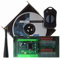
KIT RF MODULE 915MHZ FOR STK500
Manufacturer
Atmel
Series
SmartRF®r
Type
Transmitter, Receiver, ASK, FSKr
Specifications of ATAKSTK511-9
Frequency
915MHz
Wireless Frequency
915 MHz
Modulation
ASK, FSK
Operating Voltage
5 V
Antenna
External Whip
For Use With/related Products
ATSTK500
Lead Free Status / RoHS Status
Contains lead / RoHS non-compliant


4842B–AVR–10/09
STK511 Receiver Board
3.1.5
3.1.6
3.1.7
3-2
XTAL Oscillator
Signal Testpoints
Antenna Matching
The internal local oscillator (LO) for the receiver is determined by a scaled representation of the crystal
frequency. The scale factor is different for each receiver. The ATA5743 receiver uses the crystal fre-
quency times sixty-four to achieve the LO frequency. The ATA5760 and ATA5761 both use the crystal
times 128 for the LO. This scaling factor must be taken into consideration when determining the crystal
frequency. The following illustrates how the crystal oscillator frequency can be calculated.
To determine the proper crystal frequency, subtract the intermediate frequency (IF) from the carrier fre-
quency and then divide by the scaling factor for that IC. The IF for the receivers supported by this kit is
about 1 MHz. Using the ATA5743 at a carrier frequency of 315 MHz, the crystal frequency is calculated
below.
XTAL (f)
The crystal manufacturer should specify the load capacitance for the crystal. It is recommended that the
center frequency of the crystal be verified to ensure optimal operation of the receiver. This can be done
by carefully measuring the RESET_MARKER frequency. This occurs on the DATA pin upon first applica-
tion of power and has a frequency of 1/(4096
device datasheet for more details pertaining to T
Several testpoints were included on the Receiver Application Board to provide access to key signals.
Signals accessible through testpoints are labeled Data, DCLK (DataCLK), and Polling (Enable).
The Data testpoint provides access to the main interface to the receiver IC. This is a bi-directional line
that passes data to and from the receiver. It is an open collector output on the receiver so an external
pull-up resistor is included on the Receiver Application Board.
DCLK (DataCLK) provides access to the Data Clock output from the receiver. This signal only appears
under certain conditions but can greatly reduce the software effort needed to decoding the transmission.
For the Data Clock to appear, the received RF signal must be encoded using Manchester or Bi-phase
format. These forms of encoding are unique in that the duty cycle is always 50% regardless of the bit
value transmitted. In this encoding scheme, sending sequential bits of the same value results in a square
wave with some edge-to-edge time T. When the value of the bits sent is different from the previous one,
the edge-to-edge time becomes 2T. The receiver looks for this transition from T to 2T and is able to syn-
chronize with the incoming transmission. Consequently, the receiver places Data Clock pulses on the
D_CLK line that correspond with valid demodulated data.
The Polling (Enable) testpoint is an input signal to the receiver and allows the user to quickly place the
receiver in the active mode (receiver continuously active). Asserting this signal low will cause the
receiver to enter the active receive mode. Incoming signals will be processed according to the configura-
tion set in the registers. A logic high, places the receiver in the polling mode with sleep times set by the
value in the OPMODE register.
On the Receiver Application Board, provisions have been made to match the receiver IC to an antenna.
This match may include a SAW filter in some cases. This SAW filter is not required but can be used to
achieve more image suppression. As shipped, the Receiver Application Board is matched to 50
SMA. It is intended for use with an off-the-shelf external whip antenna. An antenna with an impedance
different from this will require additional matching.
= (315 MHz – 1 MHz)/64
= 314 MHz/64
= 4.90625 MHz
CLK
T
CLK
.
), where T
CLK
is the basic clock cycle. Refer to the
STK511 User Guide
at the
Related parts for ATAKSTK511-9
Image
Part Number
Description
Manufacturer
Datasheet
Request
R

Part Number:
Description:
DEV KIT FOR AVR/AVR32
Manufacturer:
Atmel
Datasheet:

Part Number:
Description:
INTERVAL AND WIPE/WASH WIPER CONTROL IC WITH DELAY
Manufacturer:
ATMEL Corporation
Datasheet:
Part Number:
Description:
Low-Voltage Voice-Switched IC for Hands-Free Operation
Manufacturer:
ATMEL Corporation
Datasheet:
Part Number:
Description:
MONOLITHIC INTEGRATED FEATUREPHONE CIRCUIT
Manufacturer:
ATMEL Corporation
Datasheet:
Part Number:
Description:
AM-FM Receiver IC U4255BM-M
Manufacturer:
ATMEL Corporation
Datasheet:
Part Number:
Description:
Monolithic Integrated Feature Phone Circuit
Manufacturer:
ATMEL Corporation
Datasheet:
Part Number:
Description:
Multistandard Video-IF and Quasi Parallel Sound Processing
Manufacturer:
ATMEL Corporation
Datasheet:
Part Number:
Description:
High-performance EE PLD
Manufacturer:
ATMEL Corporation
Datasheet:
Part Number:
Description:
8-bit Flash Microcontroller
Manufacturer:
ATMEL Corporation
Datasheet:
Part Number:
Description:
2-Wire Serial EEPROM
Manufacturer:
ATMEL Corporation
Datasheet: