WS2512-BLK Avago Technologies US Inc., WS2512-BLK Datasheet - Page 4
WS2512-BLK
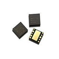
Manufacturer Part Number
WS2512-BLK
Description
MODULE PA UMTS2100 4X4MM 10-PIN
Manufacturer
Avago Technologies US Inc.
Type
Power Amplifierr
Specifications of WS2512-BLK
Package / Case
10-DFN
Current - Supply
465mA ~ 510mA
Frequency
1.92GHz ~ 1.98GHz
Gain
23.5dB ~ 26.5dB
Rf Type
W-CDMA, HSPDA
Voltage - Supply
3.2V ~ 4.2V
Operating Frequency
1980 MHz
Operating Supply Voltage
4.2 V
Supply Current
510 mA
Maximum Operating Temperature
+ 90 C
Mounting Style
SMD/SMT
Minimum Operating Temperature
- 20 C
Number Of Channels
1 Channel
Frequency (max)
1.98GHz
Power Supply Requirement
Single
Single Supply Voltage (min)
3.2V
Single Supply Voltage (typ)
3.4V
Single Supply Voltage (max)
4.2V
Package Type
SMD
Dual Supply Voltage (min)
Not RequiredV
Dual Supply Voltage (typ)
Not RequiredV
Dual Supply Voltage (max)
Not RequiredV
Operating Temperature Classification
Commercial
Operating Temp Range
-20C to 90C
Pin Count
10
Mounting
Surface Mount
Lead Free Status / RoHS Status
Lead free / RoHS Compliant
Noise Figure
-
P1db
-
Test Frequency
-
Lead Free Status / Rohs Status
Compliant
Available stocks
Company
Part Number
Manufacturer
Quantity
Price

Part Number:
WS2512-BLK
Manufacturer:
AVAGO/安华高
Quantity:
20 000


Table 4. Electrical Characteristics for WCDMA Mode (Vcc = 3.4 V, Vref = 2.85 V, T = 25 C, Zin/Zout = 50 )
Characteristics
Switching Time Low
Turn On Time
Turn Off Time
Notes:
1. Electrical characteristics are specified under WCDMA modulated (3 GPP Uplink DPCCH + 1DPDCH ) signal unless specified otherwise.
2. Control current when series 6.2 k is used.
3. ACP is expressed as a ratio of total adjacent power to signal power, both with 3.84 MHz bandwidth at specified offsets.
4. TswhighDC, TswlowDC is time required to reach stable quiescent bias (10%) after Vcont is switched low and high, respectively.
5. TonDC is time required to reach stable quiescent bias (10%) after Vref is switched high.
6. TonRF is time required to reach final output power ( 1 dB) after Vref is switched high.
Table 5. Electrical Characteristics for HSDPA Mode (Vcc = 3.4 V, Vref = 2.85 V, T = 25 C, Zin/Zout = 50 )
Characteristics
Operating Frequency Range
Gain
Power Added Efficiency
Total Supply Current
Adjacent Channel Leakage Ratio
Notes:
1. Electrical characteristics are specified under HSDPA modulated Up-Link signal (DPCCH/DPDCH = 12/15, HS-DPCCH/DPDCH = 15/15).
2. ACP is expressed as a ratio of total adjacent power to signal power, both with 3.84 MHz bandwidth at specified offsets.
4
TswhighRF, TswlowRF is time required to reach final output power ( 1 dB) after Vcont is switched low and high, respectively.
ToffRF is time required to output power to drop 30 dB after Vref is switched low.
ToffDC is time required for the current to be less than 10% of the Iq after Vref is switched low.
5 MHz offset
10 MHz offset
10 MHz offset
5 MHz offset
10 MHz offset
5 MHz offset
[5]
[6]
[4]
[2]
Symbol
F
Gain_hih
Gain_midh
Gain_lowh
PAE_hih
PAE_midh
PAE_lowh
Icc_hih
Icc_midh
Icc_lowh
ACLR1_hih
ACLR2_hih
ACLR1_midh Mid Power Mode, Pout = 16 dBm
ACLR2_midh
ACLR1_lowh Low Power Mode, Pout = 7 dBm,
ACLR2_lowh Vcc = 1.5 V
Symbol
DC
RF
DC
RF
DC
RF
Condition
TswlowDC
TswlowRF
TonDC
TonRF
ToffDC
ToffRF
Condition
High Power Mode, Pout = 27.5 dBm
Mid Power Mode, Pout = 16.0 dBm
Low Power Mode, Pout = 7.0 dBm,
Vcc = 1.5 V
High Power Mode, Pout = 27.5 dBm
Mid Power Mode, Pout = 16.0 dBm
Low Power Mode, Pout = 7.0 dBm,
Vcc = 1.5 V
High Power Mode, Pout = 27.5 dBm
Mid Power Mode, Pout = 16.0 dBm
Low Power Mode, Pout = 7.0 dBm,
Vcc = 1.5 V
High Power Mode, Pout = 27.5 dBm
Min. Typ.
–
–
–
Min.
1920
23.5
14.5
9.5
34
16.4
9.6
20
1
20
1
20
1
Typ.
–
26.5
17.5
12..5
38.8
21.7
14.3
425
53
22
-40
-55
-44
-56
-40
-56
Max. Unit
–
–
–
–
–
–
[1]
Max. Unit
1980 MHz
485
70
33
-37
-47
-37
-47
-37
-47
[1]
(cont’ d .)
s
s
s
s
s
s
dB
dB
dB
%
%
%
mA
mA
mA
dBc
dBc
dBc
dBc
dBc
Related parts for WS2512-BLK
Image
Part Number
Description
Manufacturer
Datasheet
Request
R

Part Number:
Description:
MODULE PA UMTS2100 4X4MM 10-PIN
Manufacturer:
Avago Technologies US Inc.
Datasheet:

Part Number:
Description:
OPTOCOUPLER GATE DRV 2A 16-SOIC
Manufacturer:
Avago Technologies US Inc.
Datasheet:
Part Number:
Description:
OPTOCOUPLER 2CH 2.5A 16-SOIC
Manufacturer:
Avago Technologies US Inc.
Datasheet:

Part Number:
Description:
OPTOCOUPLER GATE DRV 0.4A 16SOIC
Manufacturer:
Avago Technologies US Inc.
Datasheet:

Part Number:
Description:
OPTOCOUPLER 2.0A 250KHZ 8-DIP
Manufacturer:
Avago Technologies US Inc.
Datasheet:

Part Number:
Description:
OPTOCOUPLER 2.0A 250KHZ GW 8-SMD
Manufacturer:
Avago Technologies US Inc.
Datasheet:

Part Number:
Description:
OPTOCOUPLER 2CH 15MBD 3.3V 8SOIC
Manufacturer:
Avago Technologies US Inc.
Datasheet:
Part Number:
Description:
OPTOCOUPLER DARL-OUT 8-DIP
Manufacturer:
Avago Technologies US Inc.
Datasheet:
Part Number:
Description:
OPTOCOUPLER IGBT DRIVE 0.4A 8DIP
Manufacturer:
Avago Technologies US Inc.
Datasheet:
Part Number:
Description:
OPTOCOUPLER DARL-OUT 8-DIP
Manufacturer:
Avago Technologies US Inc.
Datasheet:

Part Number:
Description:
OPTOCOUPLER 1CH 1MBS 8-SMD GW
Manufacturer:
Avago Technologies US Inc.
Datasheet:
Part Number:
Description:
OPTOCOUPLER GATE DRIVER 8-DIP
Manufacturer:
Avago Technologies US Inc.
Datasheet:

Part Number:
Description:
OPTOCOUPLER GATE DRIVER 8-SMD
Manufacturer:
Avago Technologies US Inc.
Datasheet:

Part Number:
Description:
OPTOCOUPLER PHOTOTRANS 4-SMD
Manufacturer:
Avago Technologies US Inc.
Datasheet:

Part Number:
Description:
OPTOCOUPLER W/BASE 6-DIP
Manufacturer:
Avago Technologies US Inc.
Datasheet: