WS2512-BLK Avago Technologies US Inc., WS2512-BLK Datasheet
WS2512-BLK
Specifications of WS2512-BLK
Available stocks


Related parts for WS2512-BLK


WS2512-BLK Summary of contents
Page 1
... A low current (Vcont) pin is provided for high efficiency improvement of the low output power range. The WS2512-TR1G features CoolPAM circuit technology offering state-of-the-art reliability, temperature stability and ruggedness. The WS2512-TR1G is self contained, in- corporating 50 input and output matching networks. Functional Block Diagram RF ...
Page 2
Table 1. Absolute Maximum Ratings Parameter Symbol RF Input Power Pin DC Supply Voltage Vcc DC Reference Voltage Vref Mode Control Voltage Vcont Storage Temperature Tstg Table 2. Recommended Operating Condition Parameter Symbol DC Supply Voltage - High/Mid Power Mode ...
Page 3
Table 4. Electrical Characteristics for WCDMA Mode (Vcc = 3.4 V, Vref = 2. Zin/Zout = 50 ) Characteristics Symbol Operating Frequency Range F Gain_hi Gain Gain_mid Gain_low PAE_hi Power Added Efficiency PAE_mid PAE_low Icc_hi ...
Page 4
Table 4. Electrical Characteristics for WCDMA Mode (Vcc = 3.4 V, Vref = 2. Zin/Zout = 50 ) Characteristics Symbol DC Switching Time Low [ [5] Turn On Time RF DC [6] Turn ...
Page 5
Characteristics Data (WCDMA, Control Scheme: 3-Mode Control, Vcc = 3.4/ Vref = 2.85 V, T=25 C, Zin/Zout = 50 ) 500 450 1920 MHz 400 350 1950 MHz 300 1980 MHz 250 200 150 100 50 0 -10 ...
Page 6
Characteristics Data (WCDMA, Control Scheme: 2-Mode Control, Vcc = 3.4 V, Vref = 2.85 V, T=25 C, Zin/Zout = 50 ) 500 450 1920 MHz 400 1950 MHz 350 300 1980 MHz 250 200 150 100 50 0 -10 -5 ...
Page 7
Characteristics Data (HSDPA, Control Scheme: 3-Mode Control, Vcc = 3.4/1.5 V, Vref = 2.85 V, T=25 C, Zin/Zout = 50 ) 500 1920 MHz 450 400 1950 MHz 350 1980 MHz 300 250 200 150 100 50 0 -10 -5 ...
Page 8
Evaluation Board Descrpition Vcc1 1 Vcc1 C1 C5 100pF 2.2uF 2 RFIn GND Vcont 4 Vcont R1 C3 6.2 kohm 100pF Vref 5 Vref C4 100pF Figure 16. Evaluation board schematic Figure 17. Evaluation ...
Page 9
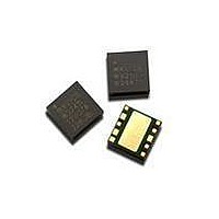
... TOP VIEW 1.2 1.9 1.7 0.85 0.85 X-RAY BOTTOM VIEW Figure 18. Package dimensional drawing and pin descriptions (all dimensions are in millimeters) PIN 1 MARK AVAGO WS2512G Manufacturing Part Number PYYWW Lot Number AAAAAG Figure 19. Marking specifications 9 0.70 TYP 0. 1.1 0.1 SIDE VIEW 1 ...
Page 10
... Use 50 transmission line between PAM and Duplexer and make it as short as possible to reduce conduction loss. • -type circuit topology is good to use for matching circuit between PA and Duplexer. • Pull-up resistor (R1) should be used to limit current drain. 6 recommended for WS2512-TR1G. Figure 20. Peripheral circuit 10 ...
Page 11
... Probability Distribution Function implies that what is important for longer talk time is the efficiency of low or medium power range rather than the efficiency at full power. WS2512-TR1G idle current and operat- ing current at 16 dBm nominal condition. Average current calculated with CDMA PDF urban area and suburban area for 2-mode control ...
Page 12
... Coupling this technology with a DC-DC converter can result in further power saving. WS2512 was developed to be compatible with a DC-DC converter serving as the DC power supply, which can improve system efficiency when lower supply voltage is adequate ...
Page 13
... PAE graphs for 2-mode control and 3-mode control are shown in Figure 27 and Figure 28. HSDPA WS2512-TR1G meets stringent HSDPA linearity require- ment up to 27dBm. WS2512-TR1G can operate dBm with Rel.99, which has a lower PAR than HSDPA. Table 7. Control Scheme: 3-Mode Control (DC-DC Converter Compatible) Power Mode High Power Mode 2 ...
Page 14
... PCB Design Guidelines The recommended WS2512-TR1G PCB land pattern is shown in Figure 29 and Figure 30. The substrate is coated with solder mask between the I/O and conductive paddle to protect the gold pads from short circuit that is caused by solder bleeding/bridging. Stencil Design Guidelines A properly designed solder screen or stencil is required to ensure optimum amount of solder paste is deposited onto the PCB pads ...
Page 15
Tape and Reel Information SECTION SECTION DIMENSIONS NOTATION MILLIMETERS A0 4.40 0.10 B0 4.40 0.10 K0 1.70 0.10 D0 1.55 0.05 D1 1.60 0.10 P0 4.00 0.10 ...
Page 16
Reel Drawing BACK VIEW FRONT VIEW Figure 33. Plastic reel format (all dimensions are in millimeters) 16 NOTES: 1. Reel shall be labeled with the following information (as a minimum): a. manufacturers name or symbol b. Agilent Technologies part number ...
Page 17
... After this time period, the part would need to be removed from the reel, detaped and then rebaked. MSL classification reflow temperature for the WS2512-TR1G is targeted at 260 C +0/-5 C. Figure 34 and Table 10 show typical SMT profile for maximum temperature of 260 +0/-5 C. ...
Page 18
max Ts min ts PREHEAT PEAK Figure 34. Typical SMT reflow profile for maximum temperature = 260 + 0/-5 C Table 10. Typical SMT Reflow Profile for Maximum Temperature = ...
Page 19
Storage Condition Packages described in this document must be stored in sealed moisture barrier, antistatic bags. Shelf life in a sealed moisture barrier bag is 12 months at <40 C and 90% relative humidity (RH) J-STD-033 p. 7. Out-of-Bag Time ...
Page 20
Table 11. Recommended Equivalent Total Floor Life (Days & for ICs with Novolac, Biphenyl and Multifunctional Epoxies (reflow at same temperature at which the component was classified) Moisture Package Type and Sensitivity Body ...