EVAL-ADM1066LFEBZ Analog Devices Inc, EVAL-ADM1066LFEBZ Datasheet - Page 6
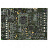
EVAL-ADM1066LFEBZ
Manufacturer Part Number
EVAL-ADM1066LFEBZ
Description
BOARD EVALUATION FOR ADM1066LF
Manufacturer
Analog Devices Inc
Specifications of EVAL-ADM1066LFEBZ
Main Purpose
Power Management, Power Supply Supervisor/Tracker/Sequencer
Embedded
No
Utilized Ic / Part
ADM1066
Primary Attributes
10 Channel Supervisor / Sequencer, 6 Voltage Output DACs
Secondary Attributes
GUI Programmable via SMBus (via USB)
Lead Free Status / RoHS Status
Lead free / RoHS Compliant


ADM1066
Parameter
BUFFERED VOLTAGE OUTPUT DACs
REFERENCE OUTPUT
PROGRAMMABLE DRIVER OUTPUTS
Conversion Time
Offset Error
Input Noise
AUX1, AUX2 Input Impedance
Resolution
Code 0x7F Output Voltage
Output Voltage Range
LSB Step Size
INL
DNL
Gain Error
Maximum Load Capacitance
Settling Time to 50 pF Load
Load Regulation
PSRR
Reference Output Voltage
Load Regulation
Minimum Load Capacitance
PSRR
Maximum Load Current (Source)
Maximum Load Current (Sink)
High Voltage (Charge-Pump)
Standard (Digital Output) Mode
Three-State Output Leakage
Oscillator Frequency
Range 1
Range 2
Range 3
Range 4
Mode (PDO1 to PDO6)
Output Impedance
V
V
V
I
(PDO1 to PDO10)
V
V
I
I
R
I
Current
OUTAVG
OL
SINK
SOURCE
OH
OH
OH
OH
OL
PULL-UP
2
2
2
(VPx)
2
2.043
Min
1
0.592
0.796
0.996
1.246
1
11
10.5
8
2.4
V
0
16
90
PU
− 0.3
Typ
0.44
84
0.25
8
0.6
0.8
1
1.25
601.25
100
100
2.5
60
40
2.048
0.25
60
500
12.5
12
10
20
20
100
2.36
−0.25
Max
±2
0.603
0.803
1.003
1.253
±0.75
±0.4
1
50
2
2.053
14
13.5
13.5
4.5
0.50
20
60
29
2
10
110
Rev. D | Page 6 of 32
ms
ms
LSB
mV
V
μF
mA
kΩ
kHz
Unit
LSB
MΩ
Bits
V
V
V
V
mV
LSB
LSB
%
μA
μA
pF
μs
mV
dB
dB
mV
mV
dB
kΩ
V
V
V
μA
V
V
V
V
mA
mA
μA
rms
Test Conditions/Comments
One conversion on one channel
All 12 channels selected, 16× averaging enabled
V
Direct input (no attenuator)
Six DACs are individually selectable for centering on one of four
output voltage ranges
Same range, independent of center point
Endpoint corrected
Per mA
DC
100 mV step in 20 ns with 50 pF load
No load
Sourcing current, I
Sinking current, I
Capacitor required for decoupling, stability
DC
I
I
I
2 V < V
V
V
V
I
Maximum sink current per PDOx pin
Maximum total sink for all PDOx pins
Internal pull-up
Current load on any VPx pull-ups, that is, total source current
available through any number of PDO pull-up switches
configured onto any one VPx pin
V
All on-chip time delays derived from this clock
OH
OH
OH
OL
REFIN
PU
PU
PU
PDO
= 20 mA
= 0 μA
= 1 μA
= 7 μA
(pull-up to VDDCAP or VPx) = 2.7 V, I
to VPx = 6.0 V, I
≤ 2.7 V, I
= 14.4 V
= 2.048 V
OH
< 7 V
OH
= 0.5 mA
DACxMAX
DACxMAX
OH
= 0 mA
= 100 μA
= −100 μA
OH
= 0.5 mA
Related parts for EVAL-ADM1066LFEBZ
Image
Part Number
Description
Manufacturer
Datasheet
Request
R

Part Number:
Description:
IC, ADJ LDO REG, 1.5V TO 5V 250mA MSOP-8
Manufacturer:
Vishay
Datasheet:

Part Number:
Description:
IC, ADJ LDO REG, 1.5V TO 5V 0.6A 8-TSSOP
Manufacturer:
Vishay
Datasheet:
Part Number:
Description:
IC, ADJ LDO REG, 1.5V TO 5V 250mA MSOP-8
Manufacturer:
Vishay
Datasheet:

Part Number:
Description:
IC ADJ LDO REG 1.5V TO 5V 150mA 5-SOT-23
Manufacturer:
Vishay
Datasheet:

Part Number:
Description:
BOARD EVAL AS1324-AD
Manufacturer:
austriamicrosystems
Datasheet:
Part Number:
Description:
IC, ADJ LDO REG, 1.5V TO 5V 0.6A 8-TSSOP
Manufacturer:
Vishay
Datasheet:

Part Number:
Description:
IC, ADJ LDO REG, 1.5V TO 5V, 0.3A, MSOP8
Manufacturer:
Vishay
Datasheet:
Part Number:
Description:
IC, ADJ LDO REG, 1.5V TO 5V, 0.3A, MSOP8
Manufacturer:
Vishay
Datasheet:
Part Number:
Description:
IC, ADJ LDO REG 1.215V TO 5V 0.3A MSOP-8
Manufacturer:
Vishay
Datasheet:
Part Number:
Description:
IC, ADJ LDO REG 1.215V TO 5V 0.3A MSOP-8
Manufacturer:
Vishay
Datasheet:

Part Number:
Description:
±1.7g Dual-Axis IMEMS Accelerometer Evaluation Board
Manufacturer:
Analog Devices Inc
Datasheet:

Part Number:
Description:
IC MULTIPLIER ANALOG 8-SOIC T/R
Manufacturer:
Analog Devices Inc
Datasheet:

Part Number:
Description:
IC ANALOG MULTIPLIER 8-DIP
Manufacturer:
Analog Devices Inc
Datasheet:
Part Number:
Description:
IC ANALOG MULTIPLIER 8-SOIC
Manufacturer:
Analog Devices Inc
Datasheet:
Part Number:
Description:
IC ANALOG MULTIPLIER 8-DIP
Manufacturer:
Analog Devices Inc
Datasheet: