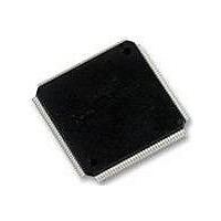
XR17D158IV-F Exar Corporation, XR17D158IV-F Datasheet - Page 46

XR17D158IV-F
Manufacturer Part Number
XR17D158IV-F
Description
IC UART PCI BUS OCTAL 144LQFP
Manufacturer
Exar Corporation
Type
IrDA or RS- 485r
Datasheet
1.XR17D158CV-F.pdf
(73 pages)
Specifications of XR17D158IV-F
Number Of Channels
8
Package / Case
144-LQFP
Features
*
Fifo's
64 Byte
Protocol
RS485
Voltage - Supply
3.3V, 5V
With Auto Flow Control
Yes
With Irda Encoder/decoder
Yes
With False Start Bit Detection
Yes
With Modem Control
Yes
Mounting Type
Surface Mount
Data Rate
6.25 Mbps
Supply Voltage (max)
5.5 V
Supply Voltage (min)
4.5 V
Supply Current
5 mA
Maximum Operating Temperature
+ 85 C
Minimum Operating Temperature
- 40 C
Mounting Style
SMD/SMT
Operating Supply Voltage
5 V
No. Of Channels
8
Uart Features
Tx/Rx FIFO Counters
Supply Voltage Range
3V To 5.5V
Operating Temperature Range
-40°C To +85°C
Digital Ic Case Style
LQFP
Rohs Compliant
Yes
Lead Free Status / RoHS Status
Lead free / RoHS Compliant
Lead Free Status / RoHS Status
Lead free / RoHS Compliant, Lead free / RoHS Compliant
Other names
1016-1292
Available stocks
Company
Part Number
Manufacturer
Quantity
Price
Company:
Part Number:
XR17D158IV-F
Manufacturer:
EXAR21
Quantity:
100
Company:
Part Number:
XR17D158IV-F
Manufacturer:
Exar Corporation
Quantity:
10 000
Part Number:
XR17D158IV-F
Manufacturer:
EXAR/艾科嘉
Quantity:
20 000
XR17D158
UNIVERSAL (3.3V AND 5V) PCI BUS OCTAL UART
The Line Control Register is used to specify the asynchronous data communication format. The word or
character length, the number of stop bits, and the parity are selected by writing the appropriate bits in this
register.
LCR[1:0]: TX and RX Word Length Select
These two bits specify the word length to be transmitted or received.
LCR[2]: TX and RX Stop-bit Length Select
The length of stop bit is specified by this bit in conjunction with the programmed word length.
LCR[3]: TX and RX Parity Select
Parity or no parity can be selected via this bit. The parity bit is a simple way used in communications for data
integrity check. See
•
•
LCR[4]: TX and RX Parity Select
If the parity bit is enabled with LCR bit-3 set to a logic 1, LCR BIT-4 selects the even or odd parity format.
•
•
LCR[5]: TX and RX Parity Select
If the parity bit is enabled, LCR BIT-5 selects the forced parity format.
•
•
•
5.8.7
Logic 0 = No parity.
Logic 1 = A parity bit is generated during the transmission while the receiver checks for parity error of the
data character received.
Logic 0 = ODD Parity is generated by forcing an odd number of logic 1’s in the transmitted character. The
receiver must be programmed to check the same format (default).
Logic 1 = EVEN Parity is generated by forcing an even the number of logic 1’s in the transmitted character.
The receiver must be programmed to check the same format.
LCR BIT-5 = logic 0, parity is not forced (default).
LCR BIT-5 = logic 1 and LCR BIT-4 = logic 0, parity bit is forced to a logical 1 for the transmit and receive
data.
LCR BIT-5 = logic 1 and LCR BIT-4 = logic 1, parity bit is forced to a logical 0 for the transmit and receive
data.
Line Control Register (LCR) - Read/Write
Table 16
for parity selection summary below.
BIT-1
BIT-2
0
0
1
1
0
1
1
LENGTH
BIT-0
5,6,7,8
W
6,7,8
0
1
0
1
ORD
5
46
S
W
TOP BIT LENGTH
(B
5 (default)
ORD LENGTH
1 (default)
IT TIME
1-1/2
6
7
8
2
(
S
))
xr
REV. 1.2.2


