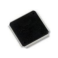
XR17D158IV-F Exar Corporation, XR17D158IV-F Datasheet - Page 33

XR17D158IV-F
Manufacturer Part Number
XR17D158IV-F
Description
IC UART PCI BUS OCTAL 144LQFP
Manufacturer
Exar Corporation
Type
IrDA or RS- 485r
Datasheet
1.XR17D158CV-F.pdf
(73 pages)
Specifications of XR17D158IV-F
Number Of Channels
8
Package / Case
144-LQFP
Features
*
Fifo's
64 Byte
Protocol
RS485
Voltage - Supply
3.3V, 5V
With Auto Flow Control
Yes
With Irda Encoder/decoder
Yes
With False Start Bit Detection
Yes
With Modem Control
Yes
Mounting Type
Surface Mount
Data Rate
6.25 Mbps
Supply Voltage (max)
5.5 V
Supply Voltage (min)
4.5 V
Supply Current
5 mA
Maximum Operating Temperature
+ 85 C
Minimum Operating Temperature
- 40 C
Mounting Style
SMD/SMT
Operating Supply Voltage
5 V
No. Of Channels
8
Uart Features
Tx/Rx FIFO Counters
Supply Voltage Range
3V To 5.5V
Operating Temperature Range
-40°C To +85°C
Digital Ic Case Style
LQFP
Rohs Compliant
Yes
Lead Free Status / RoHS Status
Lead free / RoHS Compliant
Lead Free Status / RoHS Status
Lead free / RoHS Compliant, Lead free / RoHS Compliant
Other names
1016-1292
Available stocks
Company
Part Number
Manufacturer
Quantity
Price
Company:
Part Number:
XR17D158IV-F
Manufacturer:
EXAR21
Quantity:
100
Company:
Part Number:
XR17D158IV-F
Manufacturer:
Exar Corporation
Quantity:
10 000
Part Number:
XR17D158IV-F
Manufacturer:
EXAR/艾科嘉
Quantity:
20 000
xr
REV. 1.2.2
The receiver section contains an 8-bit Receive Shift Register (RSR) and Receive Holding Register (RHR). The
RSR uses the 16X or 8X clock for timing. It verifies and validates every bit on the incoming character in the
middle of each data bit. On the falling edge of a start or false start bit, an internal receiver counter starts
counting at the 16X or 8X clock rate. After 8 or 4 clocks the start bit period should be at the center of the start
bit. At this time the start bit is sampled and if it is still a logic 0 it is validated. Evaluating the start bit in this
manner prevents the receiver from assembling a false character. The rest of the data bits and stop bits are
sampled and validated in this same manner to prevent false framing. If there were any error(s), they are
reported in the LSR register bits 1- 4. Upon unloading the receive data byte from RHR, the receive FIFO
pointer is bumped and the error flags are immediately updated to reflect the status of the data byte in RHR
register. RHR can generate a receive data ready interrupt upon receiving a character or delay until it reaches
the FIFO trigger level. Furthermore, data delivery to the host is guaranteed by a receive data ready time-out
function when receive data does not reach the receive FIFO trigger level. This time-out delay is 4 word lengths
as defined by LCR[1:0] plus 12 bits time. The RHR interrupt is enabled by IER bit-0.
The receive holding register is an 8-bit register that holds a receive data byte from the receive shift register
(RSR). It provides the receive data interface to the host processor. The host reads the receive data byte on this
register whenever a data byte is transferred from the RSR. RHR also part of the receive FIFO of 64 bytes by
11-bit wide, 3 extra bits are for the error flags to be in LSR register. When the FIFO is enabled by FCR bit-0, it
acts as the first-out register of the FIFO as new data are put over the first-in register. The receive FIFO pointer
is bumped after the RHR register is read. Also, the error flags associated with the data byte are immediately
updated onto the line status register (LSR) bits 1-4.
5.3
5.3.1
5.3.2
F
IGURE
Receiver
Receiver Operation in non-FIFO Mode
Receive Holding Register (RHR)
(8XMODE Register)
and Errors
Data Byte
16X or 8X Clock
14. R
Receive
ECEIVER
O
PERATION IN NON
LSR bits
Flags in
Error
4:2
Receive Data Shift
Register (RSR)
Holding Register
Receive Data
-FIFO M
(RHR)
33
ODE
UNIVERSAL (3.3V AND 5V) PCI BUS OCTAL UART
Validation
Data Bit
RHR Interrupt (ISR bit-2)
Receive Data Characters
RXFIFO1
XR17D158


