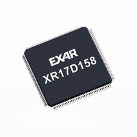
XR17D154IV-F Exar Corporation, XR17D154IV-F Datasheet - Page 5

XR17D154IV-F
Manufacturer Part Number
XR17D154IV-F
Description
IC UART PCI BUS QUAD 144LQFP
Manufacturer
Exar Corporation
Type
IrDA or RS- 485r
Datasheet
1.XR17D154CV-F.pdf
(69 pages)
Specifications of XR17D154IV-F
Number Of Channels
4, QUART
Package / Case
144-LQFP
Features
*
Fifo's
64 Byte
Protocol
RS485
Voltage - Supply
3.3V, 5V
With Auto Flow Control
Yes
With Irda Encoder/decoder
Yes
With False Start Bit Detection
Yes
With Modem Control
Yes
Mounting Type
Surface Mount
Data Rate
6.25 Mbps
Supply Voltage (max)
5.5 V
Supply Voltage (min)
3 V
Supply Current
4 mA
Maximum Operating Temperature
+ 85 C
Minimum Operating Temperature
- 40 C
Mounting Style
SMD/SMT
Operating Supply Voltage
3.3 V or 5 V
No. Of Channels
4
Uart Features
Tx/Rx FIFO Counters
Supply Voltage Range
3V To 5.5V
Operating Temperature Range
-40°C To +85°C
Digital Ic Case Style
LQFP
Rohs Compliant
Yes
Lead Free Status / RoHS Status
Lead free / RoHS Compliant
Lead Free Status / RoHS Status
Lead free / RoHS Compliant, Lead free / RoHS Compliant
Other names
1016-1290
Available stocks
Company
Part Number
Manufacturer
Quantity
Price
Company:
Part Number:
XR17D154IV-F
Manufacturer:
ADI
Quantity:
1 046
Company:
Part Number:
XR17D154IV-F
Manufacturer:
Exar Corporation
Quantity:
10 000
PIN DESCRIPTIONS
xr
REV. 1.2.2
TMRCK
MPIO1
MPIO2
MPIO3
MPIO4
MPIO5
MPIO6
MPIO7
TEST#
XTAL1
XTAL2
EEDO
EECK
EECS
N
EEDI
ENIR
VCC
AME
64, 90, 112
P
107
109
116
115
114
113
110
111
74
73
68
67
66
65
69
70
IN
#
PWR
T
I/O
I/O
I/O
I/O
I/O
I/O
I/O
YPE
O
O
O
O
I
I
I
I
I
Multi-purpose input/output 1. The function of this pin is defined thru the Con-
figuration Register MPIOSEL, MPIOLVL, MPIOINV, MPIO3T and MPIOINT.
Multi-purpose input/output 2. The function of this pin is defined thru the Con-
figuration Register MPIOSEL, MPIOLVL, MPIOINV, MPIO3T and MPIOINT.
Multi-purpose input/output 3. The function of this pin is defined thru the Con-
figuration Register MPIOSEL, MPIOLVL, MPIOINV, MPIO3T and MPIOINT.
Multi-purpose input/output 4. The function of this pin is defined thru the Con-
figuration Register MPIOSEL, MPIOLVL, MPIOINV, MPIO3T and MPIOINT.
Multi-purpose input/output 5. The function of this pin is defined thru the Con-
figuration Register MPIOSEL, MPIOLVL, MPIOINV, MPIO3T and MPIOINT.
Multi-purpose input/output 6. The function of this pin is defined thru the Con-
figuration Register MPIOSEL, MPIOLVL, MPIOINV, MPIO3T and MPIOINT.
Multi-purpose input/output 7. The function of this pin is defined thru the Con-
figuration Register MPIOSEL, MPIOLVL, MPIOINV, MPIO3T and MPIOINT.
Serial clock to EEPROM. An internal clock of CLK divide by 256 is used for
reading the vendor and sub-vendor ID and model number during power up or
reset. However, it can be manually clocked thru the Configuration Register
REGB.
Chip select to a EEPROM device like 93C46. It is manually selectable thru
the Configuration Register REGB. Requires a pull-up 4.7KΩ resistor for
external sensing of EEPROM during power up. See DAN112 for further
details.
Write data to EEPROM device. It is manually accessible thru the Configura-
tion Register REGB. The D154 auto-configuration register interface logic
uses the 16-bit format.
Read data from EEPROM device. It is manually accessible thru the Configu-
ration Register REGB.
Crystal of up to 24MHz or external clock input of up to 50MHz for data rates
up to 6.25Mbps at 5V and 8X sampling. See AC Characterization table. Cau-
tion: this input is not 5V tolerant at 3.3V.
Crystal or buffered clock output.
16-bit timer/counter external clock input.
Infrared mode enable (active high). This pin is sampled during power up, fol-
lowing a hardware reset (RST#) or soft-reset (register RESET). It can be
used to start up all 4 UARTs in the infrared mode. The sampled logic state is
transferred to MCR bit-6 in the UART. Software can override this pin thereaf-
ter and enable or disable it.
Factory Test. Connect to VCC for normal operation.
5V or 3.3V power supply for the core logic. This power supply determines
the VOH level of the non-PCI bus interface outputs. Note that VCC ≥ VIO for
normal device operation and see
VIO.
equal VIO if sleep mode is used. See Sleep Mode section on
SEE”APPLICATION EXAMPLES” ON PAGE 8.
5
UNIVERSAL (3.3V AND 5V) PCI BUS QUAD UART
D
Table 1
ESCRIPTION
for valid combinations of VCC and
However, VCC must
page
XR17D154
19.


