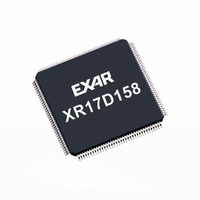
XR17D154IV-F Exar Corporation, XR17D154IV-F Datasheet - Page 37

XR17D154IV-F
Manufacturer Part Number
XR17D154IV-F
Description
IC UART PCI BUS QUAD 144LQFP
Manufacturer
Exar Corporation
Type
IrDA or RS- 485r
Datasheet
1.XR17D154CV-F.pdf
(69 pages)
Specifications of XR17D154IV-F
Number Of Channels
4, QUART
Package / Case
144-LQFP
Features
*
Fifo's
64 Byte
Protocol
RS485
Voltage - Supply
3.3V, 5V
With Auto Flow Control
Yes
With Irda Encoder/decoder
Yes
With False Start Bit Detection
Yes
With Modem Control
Yes
Mounting Type
Surface Mount
Data Rate
6.25 Mbps
Supply Voltage (max)
5.5 V
Supply Voltage (min)
3 V
Supply Current
4 mA
Maximum Operating Temperature
+ 85 C
Minimum Operating Temperature
- 40 C
Mounting Style
SMD/SMT
Operating Supply Voltage
3.3 V or 5 V
No. Of Channels
4
Uart Features
Tx/Rx FIFO Counters
Supply Voltage Range
3V To 5.5V
Operating Temperature Range
-40°C To +85°C
Digital Ic Case Style
LQFP
Rohs Compliant
Yes
Lead Free Status / RoHS Status
Lead free / RoHS Compliant
Lead Free Status / RoHS Status
Lead free / RoHS Compliant, Lead free / RoHS Compliant
Other names
1016-1290
Available stocks
Company
Part Number
Manufacturer
Quantity
Price
Company:
Part Number:
XR17D154IV-F
Manufacturer:
ADI
Quantity:
1 046
Company:
Part Number:
XR17D154IV-F
Manufacturer:
Exar Corporation
Quantity:
10 000
xr
REV. 1.2.2
N
See
See
The Baud Rate Generator (BRG) is a 16-bit counter that generates the data rate for the transmitter and
receiver. The baud rate is programmed through registers DLL and DLM which are only accessible when LCR
bit-7 is set to logic 1. See
The Interrupt Enable Register (IER) masks the interrupts from receive data ready, transmit empty, line status
and modem status registers. These interrupts are reported in the Interrupt Status Register (ISR) register and
also encoded in INT (INT0-INT3) register in the Device Configuration Registers.
IER
When the receive FIFO (FCR bit-0 = a logic 1) and receive interrupts (IER BIT-0 = logic 1) are enabled, the
RHR interrupts (see ISR bits 3 and 4) status will reflect the following:
A. The receive data available interrupts are issued to the host when the FIFO has reached the programmed
B. FIFO level will be reflected in the ISR register when the FIFO trigger level is reached. Both the ISR register
C. The receive data ready bit (LSR BIT-0) is set as soon as a character is transferred from the shift register to
IER
When FCR BIT-0 equals a logic 1 for FIFO enable, resetting IER bits 0-3 enables the 158 in the FIFO polled
mode of operation. Since the receiver and transmitter have separate bits in the LSR either or both can be used
in the polled mode by selecting respective transmit or receive control bit(s).
A. LSR BIT-0 indicates there is data in RHR or RX FIFO.
B. LSR BIT-1 indicates an overrun error has occurred and that data in the FIFO may not be valid.
C. LSR BITS 2-4 provides the type of receive data errors encountered for the data byte in RHR, if any.
D. LSR BIT-5 indicates THR is empty.
E. LSR BIT-6 indicates when both the transmit FIFO and TSR are empty.
F. LSR BIT-7 indicates a data error in at least one character in the RX FIFO.
5.8
T
5.8.1
5.8.2
5.8.3
5.8.4
A
OTE
1 1 0 0
1 1 0 0
1 1 0 1
1 1 1 0
1 1 1 1
ABLE
A3-A0
DDRESS
trigger level. It will be cleared when the FIFO drops below the programmed trigger level.
status bit and the interrupt will be cleared when the FIFO drops below the trigger level.
the receive FIFO. It is reset when the FIFO is empty.
VERSUS
VERSUS
“Section 5.3, Receiver” on page 30
“Section 5.2, Transmitter” on page 28
: MCR bits 2 and 3 (OP1 and OP2 outputs) are not available in the XR17D154. They are present for 16C550
compatibility during Internal loopback, see
13: UART CHANNEL CONFIGURATION REGISTERS DESCRIPTION.
Registers
Receive Holding Register (RHR) - Read-Only
Transmit Holding Register (THR) - Write-Only
Baud Rate Generator Divisors (DLL and DLM) - Read/Write
Interrupt Enable Register (IER) - Read/Write
XCHAR
XOFF1
XOFF2
XON1
XON2
N
R
R
R
AME
EG
ECEIVE
ECEIVE
R
W
/T
EAD
RITE
W
W
W
W
FIFO I
R
RANSMIT
/
“Section 5.1, Programmable Baud Rate Generator” on page 27
NTERRUPT
B
Bit-7
Bit-7
Bit-7
Bit-7
IT
0
-7
FIFO P
B
Bit-6
Bit-6
Bit-6
Bit-6
M
OLLED
IT
0
ODE
-6
for complete details.
O
for complete details.
M
Figure 18
PERATION
B
Bit-5
Bit-5
Bit-5
Bit-5
ODE
IT
0
-5
O
37
PERATION
.
UNIVERSAL (3.3V AND 5V) PCI BUS QUAD UART
B
Bit-4
Bit-4
Bit-4
Bit-4
IT
0
-4
B
Bit-3
Bit-3
Bit-3
Bit-3
IT
0
-3
B
Bit-2
Bit-2
Bit-2
Bit-2
IT
0
-2
S
HADED BITS ARE ENABLED BY
Xon Det.
Indicator
B
Bit-1
Bit-1
Bit-1
Bit-1
IT
-1
Xoff Det.
Indicator
for more detail.
B
Bit-0
Bit-0
Bit-0
Bit-0
IT
-0
XR17D154
EFR B
C
after read
Self-clear
OMMENT
IT
-4.


