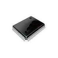
SP508CF-L Exar Corporation, SP508CF-L Datasheet - Page 22

SP508CF-L
Manufacturer Part Number
SP508CF-L
Description
IC TXRX MULTIPROTOCOL 100LQFP
Manufacturer
Exar Corporation
Type
Transceiverr
Datasheet
1.SP508CF-L.pdf
(29 pages)
Specifications of SP508CF-L
Package / Case
100-LQFP
Number Of Drivers/receivers
8/8
Protocol
Multiprotocol
Voltage - Supply
5V
Mounting Type
Surface Mount
Input Voltage Range (max)
7 V
Maximum Operating Temperature
+ 70 C
Maximum Power Dissipation
1.52 W
Minimum Operating Temperature
0 C
Mounting Style
SMD/SMT
Number Of Drivers
8
Operating Supply Voltage
5 V
Propagation Delay Time
1 us
Supply Current (max)
100 mA
Lead Free Status / RoHS Status
Lead free / RoHS Compliant
Lead Free Status / RoHS Status
Lead free / RoHS Compliant, Lead free / RoHS Compliant
Other names
1016-1192
Available stocks
Company
Part Number
Manufacturer
Quantity
Price
Company:
Part Number:
SP508CF-L
Manufacturer:
Exar Corporation
Quantity:
135
Company:
Part Number:
SP508CF-L
Manufacturer:
Exar
Quantity:
80
Part Number:
SP508CF-L
Manufacturer:
SIPEX
Quantity:
20 000
This resistor is invoked when the receiver is
operating as a V. receiver, in modes EIA-
530, EIA-530A, RS-449/V.36, and X.2. The
same receivers also incorporate a termina-
tion network internally for V.35 applications.
For V.35, the receiver input termination is a
“Y” termination consisting of two 51Ω resis-
tors connected in series and a 124Ω resistor
connected between the two 50Ω resistors
and V35RGND output. The V35RGND is
usually grounded. The receiver itself is
identical to the V. receiver.
The differential receivers can be configured
to be ITU-T-V.0 single-ended receivers
by internally connecting the non-inverting
input to ground. This is internally done
by default from the decoder. The non-in-
verting input is rerouted to V0GND and
can be grounded separately. The ITU-T-
V.0 receivers can operate over Mbps
and are used in RS-449/V.36, EA-530,
EA-530A and X.2 modes as Category II
signals as indicated by their corresponding
specifications. All receivers include an en-
able/disable line for disabling the receiver
output allowing convenient half-duplex
configurations. The enable pins will either
enable or disable the output of the receivers
according to the appropriate active logic il-
lustrated on Figure 45. The receiver’s enable
lines include an internal pull-up or pull-down
device, depending on the active polarity of
the receiver, that enables the receiver upon
power up if the enable lines are left floating.
During disabled conditions, the receiver
outputs will be at a high impedance state.
If the receiver is disabled any associated
termination is also disconnected from the
inputs.
All receivers include a fail-safe feature that
outputs a logic high when the receiver inputs
are open, terminated but open, or shorted
together. For single-ended V.28 and V.0
receivers, there are internal 5kΩ pull-down
resistors on the inputs which produces a
logic high (“”) at the receiver outputs. The
differential receivers have a proprietary cir-
cuit that detect open or shorted inputs and
if so, will produce a logic HIGH (“”) at the
receiver output.
Exar Corporation 48720 Kato Road, Fremont CA, 94538 • 50-668-707 • www.exar.com SP508_00_02709
22
ChARGE PUMP
The charge pump is a Exar-patented design
(5,306,954) and uses a unique approach
compared to older less-efficient designs.
The charge pump still requires four external
capacitors, but uses four-phase voltage
shifting technique to attain symmetrical
power supplies. The charge pump V
V
-5.8V, respectively. There is a free-running
oscillator that controls the four phases of
the voltage shifting. A description of each
phase follows.
Phase 1
__V
of the clock cycle, the positive side of capaci-
tors C
is then switched to ground and the charge
in C
nected to V
capacitor C
Phase 2
—V
nects the negative terminal of C
storage capacitor and the positive terminal
of C
generated voltage to C
voltage is regulated to –5.8V. Simultane-
ously, the positive side of the capacitor C
is switched to V
connected to ground.
Phase 3
—V
the clock is identical to the first phase—the
charge transferred in C
the negative terminal of C
to the negative side of the capacitor C
Since C
across C
Phase 4
—V
clock connects the negative terminal of C
to ground, and transfers the generated 5.8V
across C
This voltage is regulated to +5.8V. At the
regulated voltage, the internal oscillator is
disabled and simultaneously with this, the
positive side of capacitor C
V
ground, and the cycle begins again.
SS
CC
outputs are regulated to +5.8V and
and the negative side is connected to
SS
DD
DD
SS
2
- is transferred to C
to ground, and transfers the negative
transfer —Phase two of the clock con-
charge storage —The third phase of
transfer —The fourth phase of the
charge storage ——During this phase
and C
2
2
+ is at V
2
is 2
to C
2
CC
is now 2
2
are initially charged to V
, the voltage potential across
X
V
4
, the V
CC
CC
and the negative side is
.
CC
, the voltage potential
X
V
DD
2
CC
-. Since C
storage capacitor.
3
produces –V
. This generated
.
which is applied
is switched to
2
to the V
2
+ is con-
DD
CC
CC
and
. C+
in
2
SS
.
2


