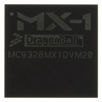
MC9328MX1DVM20 Freescale Semiconductor, MC9328MX1DVM20 Datasheet - Page 93

MC9328MX1DVM20
Manufacturer Part Number
MC9328MX1DVM20
Description
IC MCU I.MX 200MHZ 256-MAPBGA
Manufacturer
Freescale Semiconductor
Series
i.MX1r
Datasheet
1.MC9328MX1DVH20.pdf
(100 pages)
Specifications of MC9328MX1DVM20
Core Processor
ARM9
Core Size
32-Bit
Speed
200MHz
Connectivity
EBI/EMI, I²C, MMC, SmartCard, SPI, SSI, UART/USART, USB
Peripherals
DMA, I²S, LCD, POR, PWM, WDT
Number Of I /o
110
Program Memory Type
ROMless
Voltage - Supply (vcc/vdd)
1.7 V ~ 3.3 V
Oscillator Type
External
Operating Temperature
-30°C ~ 70°C
Package / Case
256-MAPBGA
Lead Free Status / RoHS Status
Lead free / RoHS Compliant
Eeprom Size
-
Ram Size
-
Program Memory Size
-
Data Converters
-
Available stocks
Company
Part Number
Manufacturer
Quantity
Price
Company:
Part Number:
MC9328MX1DVM20
Manufacturer:
Freescale Semiconductor
Quantity:
10 000
Company:
Part Number:
MC9328MX1DVM20R2
Manufacturer:
Freescale Semiconductor
Quantity:
10 000
The limitation on pixel clock rise time / fall time are not specified. It should be calculated from the hold
time and setup time, according to:
Rising-edge latch data
In most of case, duty cycle is 50 / 50, therefore
For example: Given pixel clock period = 10ns, duty cycle = 50 / 50, hold time = 1ns, setup time = 1ns.
Freescale Semiconductor
max rise time allowed = (positive duty cycle - hold time)
max fall time allowed = (negative duty cycle - setup time)
max rise time = (period / 2 - hold time)
max fall time = (period / 2 - setup time)
positive duty cycle = 10 / 2 = 5ns
=> max rise time allowed = 5 - 1 = 4ns
negative duty cycle = 10 / 2 = 5ns
=> max fall time allowed = 5 - 1 = 4ns
VSYNC
HSYNC
DATA[7:0]
PIXCLK
Ref No.
1
2
3
4
5
6
7
Figure 69. Sensor Output Data on Pixel Clock Rising Edge
csi_vsync to csi_hsync
csi_hsync to csi_pixclk
csi_d setup time
csi_d hold time
csi_pixclk high time
csi_pixclk low time
csi_pixclk frequency
Table 42. Gated Clock Mode Timing Parameters
1
CSI Latches Data on Pixel Clock Falling Edge
Parameter
MC9328MX1 Technical Data, Rev. 7
3
2
Valid Data
4
10.42
10.42
Min
180
1
1
1
0
Valid Data
Functional Description and Application Information
6
7
Max
48
–
–
–
–
–
–
5
Valid Data
MHz
Unit
ns
ns
ns
ns
ns
ns
93


