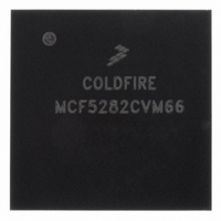
MCF5282CVM66 Freescale Semiconductor, MCF5282CVM66 Datasheet - Page 493

MCF5282CVM66
Manufacturer Part Number
MCF5282CVM66
Description
IC MPU 512K 66MHZ 256-MAPBGA
Manufacturer
Freescale Semiconductor
Series
MCF528xr
Datasheet
1.MCF5216CVM66J.pdf
(766 pages)
Specifications of MCF5282CVM66
Core Processor
Coldfire V2
Core Size
32-Bit
Speed
66MHz
Connectivity
CAN, EBI/EMI, Ethernet, I²C, SPI, UART/USART
Peripherals
DMA, LVD, POR, PWM, WDT
Number Of I /o
150
Program Memory Size
512KB (512K x 8)
Program Memory Type
FLASH
Ram Size
64K x 8
Voltage - Supply (vcc/vdd)
2.7 V ~ 3.6 V
Data Converters
A/D 8x10b
Oscillator Type
External
Operating Temperature
-40°C ~ 85°C
Package / Case
256-MAPBGA
Controller Family/series
ColdFire
No. Of I/o's
150
Ram Memory Size
64KB
Cpu Speed
66.67MHz
Embedded Interface Type
CAN, I2C, SPI, UART
No. Of Pwm Channels
8
Rohs Compliant
Yes
Lead Free Status / RoHS Status
Lead free / RoHS Compliant
Eeprom Size
-
Available stocks
Company
Part Number
Manufacturer
Quantity
Price
Company:
Part Number:
MCF5282CVM66
Manufacturer:
FREESCAL
Quantity:
152
Company:
Part Number:
MCF5282CVM66
Manufacturer:
Freescale Semiconductor
Quantity:
10 000
Part Number:
MCF5282CVM66
Manufacturer:
NXP/恩智浦
Quantity:
20 000
Company:
Part Number:
MCF5282CVM66J
Manufacturer:
Freescale Semiconductor
Quantity:
10 000
- Current page: 493 of 766
- Download datasheet (9Mb)
25.5.6
Table 25-14
25.5.7
These registers are used as acceptance masks for received frame IDs. 3 masks are defined: A global mask,
used for Rx buffers 0-13, and 2 more separate masks for buffers 14 and 15.
Mask bit = 0: The corresponding incoming ID bit is “don’t care”.
Mask bit = 1: The corresponding ID bit is checked against the incoming ID bit, to see if a match exists.
Note that these masks are used both for Standard and Extended ID formats. The value of mask registers
should NOT be changed while in normal operation, as locked frames which matched a MB through a mask,
may be transferred into the MB (upon release) but may no longer match.
Freescale Semiconductor
15–0
Bits
Bits
5–3
2–0
Address
Reset
Field
R/W
TIMER The free running timer counter can be read and written by the CPU. The timer starts from zero after
PSEG
PSEG
Name
Free Running Timer (TIMER)
Name
Rx Mask Registers
describes the TIMER fields.
1
2
PSEG1[2:0] — Phase buffer segment 1. The PSEG1 field defines the length of phase buffer segment
1 in the bit time. The valid programmed values are 0 through 7.
The length of phase buffer segment 1 is calculated as follows:
PSEG2 — Phase Buffer Segment 2. The PSEG2 field defines the length of phase buffer segment 2
in the bit time. The valid programmed values are 0 through 7.
The length of phase buffer segment 2 is calculated as follows:
reset, counts linearly to 0xFFFF, and wraps around.
The timer is clocked by the FlexCAN bit-clock. During a message, it increments by one for each bit
that is received or transmitted. When there is no message on the bus, it increments at the nominal bit
rate.
The timer value is captured at the beginning of the identifier field of any frame on the CAN bus. The
captured value is written into the “time stamp” entry in a message buffer after a successful reception
or transmission of a message.
15
Phase Buffer Segment 1 = (PSEG1 + 1) Time Quanta
Phase Buffer Segment 2 = (PSEG2 + 1) Time Quanta
MCF5282 and MCF5216 ColdFire Microcontroller User’s Manual, Rev. 3
Table 25-13. CANCTRL2 Field Descriptions (continued)
Figure 25-11. Free Running Timer (TIMER)
Table 25-14. TIMER Field Descriptions
0000_0000_0000_0000
IPSBAR + 0x1C_000A
Description
Description
TIMER
R/W
0
FlexCAN
25-23
Related parts for MCF5282CVM66
Image
Part Number
Description
Manufacturer
Datasheet
Request
R
Part Number:
Description:
Mcf5282 And Mcf5216 Coldfire Microcontroller User�s Manual
Manufacturer:
Freescale Semiconductor, Inc
Datasheet:
Part Number:
Description:
Manufacturer:
Freescale Semiconductor, Inc
Datasheet:
Part Number:
Description:
Manufacturer:
Freescale Semiconductor, Inc
Datasheet:
Part Number:
Description:
Manufacturer:
Freescale Semiconductor, Inc
Datasheet:
Part Number:
Description:
Manufacturer:
Freescale Semiconductor, Inc
Datasheet:
Part Number:
Description:
Manufacturer:
Freescale Semiconductor, Inc
Datasheet:
Part Number:
Description:
Manufacturer:
Freescale Semiconductor, Inc
Datasheet:
Part Number:
Description:
Manufacturer:
Freescale Semiconductor, Inc
Datasheet:
Part Number:
Description:
Manufacturer:
Freescale Semiconductor, Inc
Datasheet:
Part Number:
Description:
Manufacturer:
Freescale Semiconductor, Inc
Datasheet:
Part Number:
Description:
Manufacturer:
Freescale Semiconductor, Inc
Datasheet:
Part Number:
Description:
Manufacturer:
Freescale Semiconductor, Inc
Datasheet:
Part Number:
Description:
Manufacturer:
Freescale Semiconductor, Inc
Datasheet:
Part Number:
Description:
Manufacturer:
Freescale Semiconductor, Inc
Datasheet:
Part Number:
Description:
Manufacturer:
Freescale Semiconductor, Inc
Datasheet:


