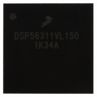
DSP56311VL150 Freescale Semiconductor, DSP56311VL150 Datasheet - Page 73

DSP56311VL150
Manufacturer Part Number
DSP56311VL150
Description
IC DSP 24BIT FIXED POINT 196-BGA
Manufacturer
Freescale Semiconductor
Series
DSP563xxr
Type
Fixed Pointr
Datasheet
1.DSP56311VL150R2.pdf
(96 pages)
Specifications of DSP56311VL150
Interface
Host Interface, SSI, SCI
Clock Rate
150MHz
Non-volatile Memory
ROM (576 B)
On-chip Ram
384kB
Voltage - I/o
3.30V
Voltage - Core
1.80V
Operating Temperature
-40°C ~ 100°C
Mounting Type
Surface Mount
Package / Case
196-MAPBGA
Package
196MA-BGA
Numeric And Arithmetic Format
Fixed-Point
Maximum Speed
150 MHz
Ram Size
384 KB
Device Million Instructions Per Second
150 MIPS
Lead Free Status / RoHS Status
Lead free / RoHS Compliant
Available stocks
Company
Part Number
Manufacturer
Quantity
Price
Company:
Part Number:
DSP56311VL150
Manufacturer:
FREESCALE
Quantity:
201
Company:
Part Number:
DSP56311VL150
Manufacturer:
MOTOLOLA
Quantity:
1 045
Company:
Part Number:
DSP56311VL150
Manufacturer:
Freescale Semiconductor
Quantity:
10 000
Part Number:
DSP56311VL150
Manufacturer:
FREESCALE
Quantity:
20 000
Company:
Part Number:
DSP56311VL150B1
Manufacturer:
ST
Quantity:
101
Company:
Part Number:
DSP56311VL150B1
Manufacturer:
Freescale Semiconductor
Quantity:
10 000
Company:
Part Number:
DSP56311VL150R2
Manufacturer:
Freescale Semiconductor
Quantity:
10 000
4.3 Power Consumption Considerations
Power dissipation is a key issue in portable DSP applications. Some of the factors affecting current consumption
are described in this section. Most of the current consumed by CMOS devices is alternating current (ac), which is
charging and discharging the capacitances of the pins and internal nodes. Current consumption is described by this
formula:
Freescale Semiconductor
For a Port A address pin loaded with 50 pF capacitance, operating at 3.3 V, with a 66 MHz clock, toggling at its maximum possible rate (33
MHz), the current consumption is expressed in Equation 4.
•
•
•
•
•
•
•
•
Where:
Because the DSP output signals have fast rise and fall times, PCB trace lengths should be minimal. This
recommendation particularly applies to the address and data buses as well as the
TA
Consider all device loads as well as parasitic capacitance due to PCB traces when you calculate
capacitance. This is especially critical in systems with higher capacitive loads that could create higher
transient currents in the
All inputs must be terminated (that is, not allowed to float) by CMOS levels except for the three pins with
internal pull-up resistors (
Take special care to minimize noise levels on the
The following pins must be asserted during power-up:
supplied before deassertion of
other “required
uninitialized state that may result in significant power consumption and heat-up. Designs should minimize
this condition to the shortest possible duration.
Ensure that during power-up, and throughout the DSP56311 operation, V
the V
If multiple DSP devices are on the same board, check for cross-talk or excessive spikes on the supplies due
to synchronous operation of the devices.
The Port A data bus (
last output value even when the internal signal is tri-stated. Typically, no pull-up or pull-down resistors
should be used with these signal lines. However, if the DSP is connected to a device that requires pull-up
resistors (such as an MPC8260), the recommended resistor value is 10 KΩ or less. If more than one DSP
must be connected in parallel to the other device, the pull-up resistor value requirement changes as
follows:
— 2 DSPs = 7 KΩ or less
— 3 DSPs = 4 KΩ or less
— 4 DSPs = 3 KΩ or less
— 5 DSPs = 2 KΩ or less
— 6 DSPs = 1.5 KΩ or less
C
V
f
Equation 3:
, and
CC
BG
voltage level.
pins. Maximum PCB trace lengths on the order of 6 inches are recommended.
=
=
=
RESET
I
=
C
D[0–23]
×
duration” conditions are met (see Table 2-7), the device circuitry can be in an
V
V
node/pin capacitance
voltage swing
frequency of node/pin toggle
CC
TRST
×
f
), HI08, ESSI0, ESSI1, SCI, and timers all use internal keepers to maintain the
and
Example 4-1. Current Consumption
RESET
,
TMS
GND
DSP56311 Technical Data, Rev. 8
,
. If the V
circuits.
DE
).
CC
V
reaches the required level before EXTAL is stable or
CCP
,
RESET
GND
P
, and
and
TRST
GND
Power Consumption Considerations
P1
. A stable
CCQH
pins.
is always higher or equal to
IRQA
EXTAL
,
IRQB
signal should be
,
IRQC
,
IRQD
4-3
,


