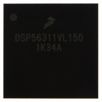
DSP56311VL150 Freescale Semiconductor, DSP56311VL150 Datasheet - Page 24

DSP56311VL150
Manufacturer Part Number
DSP56311VL150
Description
IC DSP 24BIT FIXED POINT 196-BGA
Manufacturer
Freescale Semiconductor
Series
DSP563xxr
Type
Fixed Pointr
Datasheet
1.DSP56311VL150R2.pdf
(96 pages)
Specifications of DSP56311VL150
Interface
Host Interface, SSI, SCI
Clock Rate
150MHz
Non-volatile Memory
ROM (576 B)
On-chip Ram
384kB
Voltage - I/o
3.30V
Voltage - Core
1.80V
Operating Temperature
-40°C ~ 100°C
Mounting Type
Surface Mount
Package / Case
196-MAPBGA
Package
196MA-BGA
Numeric And Arithmetic Format
Fixed-Point
Maximum Speed
150 MHz
Ram Size
384 KB
Device Million Instructions Per Second
150 MIPS
Lead Free Status / RoHS Status
Lead free / RoHS Compliant
Available stocks
Company
Part Number
Manufacturer
Quantity
Price
Company:
Part Number:
DSP56311VL150
Manufacturer:
FREESCALE
Quantity:
201
Company:
Part Number:
DSP56311VL150
Manufacturer:
MOTOLOLA
Quantity:
1 045
Company:
Part Number:
DSP56311VL150
Manufacturer:
Freescale Semiconductor
Quantity:
10 000
Part Number:
DSP56311VL150
Manufacturer:
FREESCALE
Quantity:
20 000
Company:
Part Number:
DSP56311VL150B1
Manufacturer:
ST
Quantity:
101
Company:
Part Number:
DSP56311VL150B1
Manufacturer:
Freescale Semiconductor
Quantity:
10 000
Company:
Part Number:
DSP56311VL150R2
Manufacturer:
Freescale Semiconductor
Quantity:
10 000
Specifications
2.4 AC Electrical Characteristics
The timing waveforms shown in the AC electrical characteristics section are tested with a V
and a V
Table 2-2. AC timing specifications, which are referenced to a device input signal, are measured in production with
respect to the 50 percent point of the respective input signal’s transition. DSP56311 output levels are measured
with the production test machine V
Note: Although the minimum value for the frequency of EXTAL is 0 MHz, the device AC test conditions are 15
2.4.1
2-4
Internal operation frequency with PLL
enabled
Internal operation frequency with PLL
disabled
Internal clock high period
•
•
•
Internal clock low period
•
•
•
Internal clock cycle time with PLL enabled
Internal clock cycle time with PLL disabled
Instruction cycle time
Notes:
With PLL disabled
With PLL enabled and MF ≤ 4
With PLL enabled and MF > 4
With PLL disabled
With PLL enabled and
MF ≤ 4
With PLL enabled and
MF > 4
IH
MHz and rated speed.
1.
2.
minimum of 2.4 V for all pins except EXTAL, which is tested using the input levels shown in Note 6 of
Characteristics
Internal Clocks
DF = Division Factor; Ef = External frequency; ET
PDF = Predivision Factor; T
See the PLL and Clock Generation section in the DSP56300 Family Manual for a details on the PLL.
OL
C
= internal clock cycle.
and V
Symbol
DSP56311 Technical Data, Rev. 8
I
CYC
T
T
T
T
Table 2-4.
f
f
H
C
C
L
OH
reference levels set at 0.4 V and 2.4 V, respectively.
C
PDF × DF/MF
PDF × DF/MF
PDF × DF/MF
PDF × DF/MF
0.49 × ET
0.47 × ET
0.49 × ET
0.47 × ET
= External clock cycle; MF = Multiplication Factor;
Internal Clocks
Min
—
—
—
—
—
—
—
C
C
C
C
×
×
×
×
ET
Expression
(PDF × DF)
(Ef × MF)/
2 × ET
C
DF/MF
Typ
ET
ET
× PDF ×
Ef/2
T
—
—
—
—
C
C
C
C
Freescale Semiconductor
IL
maximum of 0.3 V
PDF × DF/MF
PDF × DF/MF
PDF × DF/MF
PDF × DF/MF
0.51 × ET
0.53 × ET
0.51 × ET
0.53 × ET
Max
—
—
—
—
—
—
—
C
C
C
C
×
×
×
×


