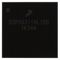
DSP56311VL150 Freescale Semiconductor, DSP56311VL150 Datasheet - Page 32

DSP56311VL150
Manufacturer Part Number
DSP56311VL150
Description
IC DSP 24BIT FIXED POINT 196-BGA
Manufacturer
Freescale Semiconductor
Series
DSP563xxr
Type
Fixed Pointr
Datasheet
1.DSP56311VL150R2.pdf
(96 pages)
Specifications of DSP56311VL150
Interface
Host Interface, SSI, SCI
Clock Rate
150MHz
Non-volatile Memory
ROM (576 B)
On-chip Ram
384kB
Voltage - I/o
3.30V
Voltage - Core
1.80V
Operating Temperature
-40°C ~ 100°C
Mounting Type
Surface Mount
Package / Case
196-MAPBGA
Package
196MA-BGA
Numeric And Arithmetic Format
Fixed-Point
Maximum Speed
150 MHz
Ram Size
384 KB
Device Million Instructions Per Second
150 MIPS
Lead Free Status / RoHS Status
Lead free / RoHS Compliant
Available stocks
Company
Part Number
Manufacturer
Quantity
Price
Company:
Part Number:
DSP56311VL150
Manufacturer:
FREESCALE
Quantity:
201
Company:
Part Number:
DSP56311VL150
Manufacturer:
MOTOLOLA
Quantity:
1 045
Company:
Part Number:
DSP56311VL150
Manufacturer:
Freescale Semiconductor
Quantity:
10 000
Part Number:
DSP56311VL150
Manufacturer:
FREESCALE
Quantity:
20 000
Company:
Part Number:
DSP56311VL150B1
Manufacturer:
ST
Quantity:
101
Company:
Part Number:
DSP56311VL150B1
Manufacturer:
Freescale Semiconductor
Quantity:
10 000
Company:
Part Number:
DSP56311VL150R2
Manufacturer:
Freescale Semiconductor
Quantity:
10 000
Specifications
2-12
Notes:
No.
111
112
113
114
115
116
117
118
119
WR deassertion to data high impedance
Previous RD deassertion to data active (write)
RD deassertion time
WR deassertion time
Address valid to RD assertion
RD assertion pulse width
RD deassertion to address not valid
TA set-up before RD or WR deassertion
TA hold after RD or WR deassertion
1.
2.
3.
4.
5.
WS is the number of wait states specified in the BCR. The value is given for the minimum for a given category. (For example,
for a category of [2 ≤ WS ≤ 7] timing is specified for 2 wait states.) Two wait states is the minimum otherwise.
Timings 100 and107 are guaranteed by design, not tested.
All timings for 150 MHz are measured from 0.5 × V
The WS number applies to the access in which the deassertion of WR occurs and assumes the next access uses a minimal
number of wait states.
Timing 118 is relative to the deassertion edge of RD or WR even if TA remains asserted.
Characteristics
4
Table 2-8.
5
DSP56311 Technical Data, Rev. 8
SRAM Timing (Continued)
CCQH
Symbol
—
—
—
—
—
—
—
—
—
to 0.5 × V
CCQH
(WS + 0.25) × T
.
0.25 × T
1.25 × T
2.25 × T
2.25 × T
3.25 × T
1.75 × T
2.75 × T
Expression
1.5 × T
2.5 × T
0.5 × T
[2 ≤ WS ≤ 7]
[2 ≤ WS ≤ 7]
[2 ≤ WS ≤ 7]
[2 ≤ WS ≤ 7]
[2 ≤ WS ≤ 7]
2.25 × T
1.25 × T
[WS ≥ 8]
[WS ≥ 8]
[WS ≥ 8]
[WS ≥ 8]
[WS ≥ 8]
C
C
C
C
C
C
C
C
C
C
− 4.0
− 4.0
− 2.8
+
−
−
− 4.0
− 4.0
− 4.0
− 4.0
C
C
4.0
4.0
1.5
C
1
− 4.0
Freescale Semiconductor
Min
11.0
17.7
14.3
12.7
11.0
11.0
7.6
6.0
0.5
4.3
3.2
—
—
0
150 MHz
Max
15.0
8.3
—
—
—
—
—
—
—
—
—
—
—
—
Unit
ns
ns
ns
ns
ns
ns
ns
ns
ns
ns
ns
ns
ns
ns


