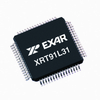
XRT91L31IQ-F Exar Corporation, XRT91L31IQ-F Datasheet - Page 26

XRT91L31IQ-F
Manufacturer Part Number
XRT91L31IQ-F
Description
IC TXRX SONET/SDH 8BIT 64QFP
Manufacturer
Exar Corporation
Type
Transceiverr
Datasheet
1.XRT91L31IQ-F.pdf
(41 pages)
Specifications of XRT91L31IQ-F
Package / Case
64-QFP
Input
LVCMOS, LVPECL, LVTTL
Output
LVCMOS, LVPECL, LVTTL
Frequency - Max
77.76MHz
Voltage - Supply
3.135 V ~ 3.465 V
Operating Temperature
-40°C ~ 85°C
Mounting Type
Surface Mount
Frequency-max
77.76MHz
Product
Framer
Number Of Transceivers
1
Data Rate
155.52 Mbps
Supply Voltage (max)
3.465 V
Supply Voltage (min)
3.135 V
Supply Current (max)
240 mA or 270 mA
Maximum Operating Temperature
+ 85 C
Minimum Operating Temperature
- 40 C
Mounting Style
SMD/SMT
Lead Free Status / RoHS Status
Lead free / RoHS Compliant
Lead Free Status / RoHS Status
Lead free / RoHS Compliant, Lead free / RoHS Compliant
Other names
1016-1361
Available stocks
Company
Part Number
Manufacturer
Quantity
Price
Company:
Part Number:
XRT91L31IQ-F
Manufacturer:
PHILIPS
Quantity:
23
Company:
Part Number:
XRT91L31IQ-F
Manufacturer:
Exar Corporation
Quantity:
10 000
Part Number:
XRT91L31IQ-F
Manufacturer:
EXAR/艾科嘉
Quantity:
20 000
XRT91L31
STS-12/STM-4 OR STS-3/STM-1 SONET/SDH TRANSCEIVER
To decouple transmit parallel clock domains of the framer/mapper device and the XRT91L31 transceiver and to
eliminate difficult timing issues between them, the transmit parallel clock TXPCLK_IO can also be optionally
configured as a clock input. Rather than provide a transmit parallel clock output reference to the framer/mapper
device, the XRT91L31 can instead accept a reference transmit parallel clock input signal from the framer/
mapper device to sample the transmit parallel bus. When PIO_CTRL pin 48 is asserted "Low," TXPCLK_IO
switches into a clock input and the XRT91L31 will now sample data on the transmit parallel bus TXDI[7:0]
based on TXPCLK_IO clock input reference coming from the framer/mapper device. The use of the alternate
transmit parallel bus clock input option permits the system to tolerate an arbitrary amount of phase mismatch
and jitter between framer/mapper transmit parallel clock timing and transceiver transmit timing.
provides a detailed overview of the alternate transmit parallel bus clock input system interface.
When applying parallel data input to the transmitter in the alternate transmit parallel bus clock input mode of
operation, the setup and hold times should be followed as shown in
F
F
3.3
3.4
IGURE
IGURE
Transmit Parallel
Framer/Mapper
Clock driven by
TXPCLK_IO
TXDI[7:0]
14. A
13. A
Alternate Transmit Parallel Bus Clock Input Option
Alternate Transmit Parallel Data Input Timing
Device
LTERNATE
LTERNATE
T
T
RANSMIT
RANSMIT
SONET Framer/ASIC
P
P
ARALLEL
ARALLEL
Alternate Transmit Parallel Clock Input Option
t
TXDI_SU
I
I
NPUT
NPUT
TXDI[7:0]
TXPCLK_IO
(Parallel Clock Input Option)
t
TXPCLK_IO
T
I
NTERFACE
IMING
8
26
B
PIO_CTRL
LOCK
TTLREFCLK
Figure 14
(P
STS-12/STM-4
t
STS-3/STM-1
TXDI_HD
Transceiver
XRT91L31
ARALLEL
REFCLKP
or
REFCLKN
CMUREFSEL
and
C
LOCK
Table
I
NPUT
14,
Table
O
PTION
15.
Figure 13
REV. 1.0.2
)


