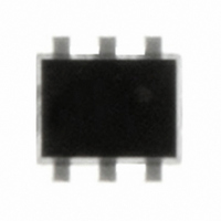
USBLC6-2P6 STMicroelectronics, USBLC6-2P6 Datasheet - Page 9

USBLC6-2P6
Manufacturer Part Number
USBLC6-2P6
Description
IC ESD PROTECTION HS SOT-666
Manufacturer
STMicroelectronics
Datasheet
1.USBLC6-2P6.pdf
(14 pages)
Specifications of USBLC6-2P6
Voltage - Working
5V
Voltage - Clamping
6V
Technology
Mixed Technology
Number Of Circuits
2
Applications
USB
Package / Case
SC-89-6, SOT-563F, SOT-666
Polarity
Bidirectional
Channels
2 Channels
Clamping Voltage
17 V
Operating Voltage
5 V
Breakdown Voltage
6 V
Termination Style
SMD/SMT
Peak Surge Current
5 A
Capacitance
3.5 pF
Maximum Operating Temperature
+ 125 C
Minimum Operating Temperature
- 40 C
Dimensions
1.7 mm W x 1.7 mm L x 0.6 mm H
Diode Type
Low Capacitance / ESD Protection
Clamping Voltage Vc Max
17V
Diode Case Style
SOT-666
No. Of Pins
6
Rohs Compliant
Yes
Operating Temperature Min Deg. C
-40C
Operating Temperature Max Deg. C
125C
Lead Free Status / RoHS Status
Lead free / RoHS Compliant
Power (watts)
-
Lead Free Status / Rohs Status
Lead free / RoHS Compliant
Other names
497-5026-2
Available stocks
Company
Part Number
Manufacturer
Quantity
Price
Company:
Part Number:
USBLC6-2P6
Manufacturer:
Keystone
Quantity:
30 000
Part Number:
USBLC6-2P6
Manufacturer:
ST
Quantity:
20 000
USBLC6-2
2.6
Figure 16. PSpice model
Note:
Figure 17. PSpice parameters
CJ0
D+in
GND
D-in
IBV
RS
BV
TT
VJ
M
0.3333
Dlow
0.9p
0.1u
1m
0.2
0.6
50
PSpice model
Figure 16.
defined by the PSpice parameters given in
This simulation model is available only for an ambient temperature of 27 °C.
LGND
LI/O
LI/O
0.3333
Dhigh
2.0p
0.52
0.1u
1m
0.6
50
shows the PSpice model of one USBLC6-2 cell. In this model, the diodes are
RGND
Dzener
0.3333
RI/O
RI/O
0.84
0.1u
40p
1m
7.3
0.6
RGND
LGND
MODEL = Dlow
RI/O
LI/O
MODEL = Dlow
110m
750p
550p
60m
MODEL = Dzener
Figure 18. USBLC6-2 PCB layout
D+in
GND
D-in
MODEL = Dhigh
MODEL = Dhigh
Figure 17.
1
considerations
USBLC6-2
RI/O
RI/O
RI/O
Technical information
LI/O
LI/O
D+out
V
D-out
LI/O
BUS
C
BUS
= 100nF
D+out
VBUS
D-out
9/14


