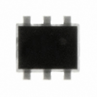
USBLC6-2P6 STMicroelectronics, USBLC6-2P6 Datasheet - Page 5

USBLC6-2P6
Manufacturer Part Number
USBLC6-2P6
Description
IC ESD PROTECTION HS SOT-666
Manufacturer
STMicroelectronics
Datasheet
1.USBLC6-2P6.pdf
(14 pages)
Specifications of USBLC6-2P6
Voltage - Working
5V
Voltage - Clamping
6V
Technology
Mixed Technology
Number Of Circuits
2
Applications
USB
Package / Case
SC-89-6, SOT-563F, SOT-666
Polarity
Bidirectional
Channels
2 Channels
Clamping Voltage
17 V
Operating Voltage
5 V
Breakdown Voltage
6 V
Termination Style
SMD/SMT
Peak Surge Current
5 A
Capacitance
3.5 pF
Maximum Operating Temperature
+ 125 C
Minimum Operating Temperature
- 40 C
Dimensions
1.7 mm W x 1.7 mm L x 0.6 mm H
Diode Type
Low Capacitance / ESD Protection
Clamping Voltage Vc Max
17V
Diode Case Style
SOT-666
No. Of Pins
6
Rohs Compliant
Yes
Operating Temperature Min Deg. C
-40C
Operating Temperature Max Deg. C
125C
Lead Free Status / RoHS Status
Lead free / RoHS Compliant
Power (watts)
-
Lead Free Status / Rohs Status
Lead free / RoHS Compliant
Other names
497-5026-2
Available stocks
Company
Part Number
Manufacturer
Quantity
Price
Company:
Part Number:
USBLC6-2P6
Manufacturer:
Keystone
Quantity:
30 000
Part Number:
USBLC6-2P6
Manufacturer:
ST
Quantity:
20 000
USBLC6-2
2.3
Figure 7.
We can significantly reduce this phenomena with simple layout optimization. It is for this
reason that some recommendations have to be followed (see
protection).
Figure 6.
How to ensure good ESD protection
While the USBLC6-2 provides high immunity to ESD surge, efficient protection depends on
the layout of the board. In the same way, with the rail to rail topology, the track from data
lines to I/O pins, from V
possible to avoid overvoltages due to parasitic phenomena (see
layout consideration)
ESD behavior: layout optimization
Unsuitable layout
Optimized layout
1 1
1 1
2
3
2
3
V
V
V
CL
CL-
ESD surge on data line
TRANSIL
+ = V
ESD behavior: parasitic phenomena due to unsuitable layout
= -V - L
TRANSIL
F
=
L
I/O
I/O
V
BR
I/O pin
6
5
4
6
5
4
di
dt
+ V + L
+
CC
Rd.Ip
L
- L
F
I/O
GND
dt
di
to V
I/O
L
L
dt
V
di
VBUS
GND
F
di
dt
BUS
+ L
V
GND
GND pin
CC
V
L
pin and from GND plane to GND pin must be as short as
TRANSIL
GND
pin
di
dt
di
dt
Figure 8.
surge > 0
surge > 0
V
CL
V
Data line
BUS
ESD SURGE
L
-L
I/O
I/O
V
ESD behavior: measurement
conditions
di
dt
di
dt
TRANSIL
+ L
- L
GND
GND
+ V
- V
di
dt
di
dt
F
IN
F
TEST BOARD
2.3: How to ensure good ESD
t = 1 ns
t = 1 ns
r
r
V
V
CL-
CL+
Figure 6.
Technical information
Negative
Positive
OUT
Surge
Surge
and
Figure 7.
t
t
+5 V
5/14
for


