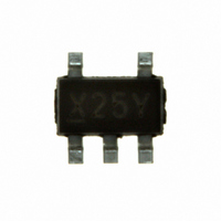
PQ1X251M2ZPH Sharp Microelectronics, PQ1X251M2ZPH Datasheet - Page 2

PQ1X251M2ZPH
Manufacturer Part Number
PQ1X251M2ZPH
Description
IC REG LDO 2.5V 150MA SOT-23-5
Manufacturer
Sharp Microelectronics
Specifications of PQ1X251M2ZPH
Regulator Topology
Positive Fixed
Voltage - Output
2.5V
Voltage - Input
Up to 9V
Voltage - Dropout (typical)
0.2V @ 150mA
Number Of Regulators
1
Current - Output
150mA (Max)
Current - Limit (min)
180mA
Operating Temperature
-30°C ~ 85°C
Mounting Type
Surface Mount
Package / Case
SOT-23-5, SC-74A, SOT-25
Number Of Outputs
1
Polarity
Positive
Input Voltage Max
9 V
Output Voltage
2.5 V
Output Type
Fixed
Dropout Voltage (max)
0.26 V at 60 mA
Output Current
0.18 A
Line Regulation
20 mV
Load Regulation
160 mV
Maximum Power Dissipation
0.35 W
Maximum Operating Temperature
+ 80 C
Mounting Style
SMD/SMT
Minimum Operating Temperature
- 30 C
Lead Free Status / RoHS Status
Lead free / RoHS Compliant
Other names
425-2329-2
Available stocks
Company
Part Number
Manufacturer
Quantity
Price
Company:
Part Number:
PQ1X251M2ZPH
Manufacturer:
SHARP
Quantity:
16 950
Company:
Part Number:
PQ1X251M2ZPH
Manufacturer:
FCI
Quantity:
22 419
Part Number:
PQ1X251M2ZPH
Manufacturer:
SHARP
Quantity:
20 000
Electrical Characteristics
Table.1 Output Voltage
Fig.1 Test Circuit
4
5
8
6
PQ1X151M2ZPH
PQ1X181M2ZPH
PQ1X251M2ZPH
PQ1X261M2ZPH
PQ1X271M2ZPH
PQ1X281M2ZPH
PQ1X291M2ZPH
PQ1X301M2ZPH
PQ1X331M2ZPH
PQ1X351M2ZPH
PQ1X371M2ZPH
PQ1X401M2ZPH
PQ1X451M2ZPH
PQ1X501M2ZPH
Output voltage
Input voltage
Output peak current
Recommended output current
Load regulation
Line regulation
Temperature coefficient of output voltage
Ripple rejection
Output noise voltage
Dropout voltage
ON-state voltage for control
ON-state current for control
OFF-state voltage for control
Quiescent current
Output OFF-state dissipation current
I
q
4 Applied to PQ1X151M2ZPH and PQ1X181M2ZPH
5 Output current shall be the value when output voltage lowers 0.3V from the voltage at I
6 Excluding PQ1X151M2ZPH and PQ1X181M2ZPH
7 Input voltage when output voltage falls 0.1V from that at Vin=Vo(TYP)+1.0V.
8 In case that the control terminal ( ③ pin) is open, output voltage should be OFF state.
, I
Model No.
qs
V
(V
IN
IN
A
=V
Parameter
O
(TYP)+1.0V, I
Symbol MIN.
V
1μF
O
1.440
1.740
2.440
2.540
2.640
2.740
2.840
2.940
3.234
3.430
3.626
3.920
4.410
4.900
O
=30mA, V
V
C
TYP.
4.0
1.5
1.8
2.5
2.6
2.7
2.8
2.9
3.0
3.3
3.5
3.7
4.5
5.0
A
Vno(rms)
Symbol
C
V
V
R
R
R
T
I
=1.8V, Ta=25°C)
V
V
R
C(ON)
C(OFF)
I
V
V
RR
C(ON)
I
eg
eg
eg
C
C (ON)
I
I-O
I-O
I
op
-
qs
eg
1.560
1.860
2.560
2.660
2.760
2.860
2.960
3.060
3.366
3.570
3.774
4.080
4.590
5.100
MAX.
O
IN
V
q
L1
L2
L3
1
2
I
O
1
2
3
10Hz<f<100kHz, C
V
IN
Unit
=V
V
I
O
O
(TYP)+1V to V
=10mA, Tj=-25 to +75°C
Io=5 to 100mA
Io=5 to 150mA
Io=5 to 60mA
Refer to Fig.2
Conditions
I
5
4
(Unless otherwise specified,V
I
O
0.01μF
V
V
O
I
=150mA
O
=60mA
C
C
2
=0mA
=1.8V
=0.2V
-
-
-
-
-
-
O
O
n
=30mA.
F=0.1μF, I
(TYP)+6V(MAX.9.0V)
Table.2 Output Noise Voltage
4.7μF
7
(V
PQ1X151M2ZPH
PQ1X181M2ZPH
PQ1X251M2ZPH
PQ1X261M2ZPH
PQ1X271M2ZPH
PQ1X281M2ZPH
PQ1X291M2ZPH
PQ1X301M2ZPH
PQ1X331M2ZPH
PQ1X351M2ZPH
PQ1X371M2ZPH
PQ1X401M2ZPH
PQ1X451M2ZPH
PQ1X501M2ZPH
7
IN
=V
Model No.
O
O
(TYP)+1.0V, I
=30mA
A
IN
=V
R
O
MIN.
180
2.3
1.8
=30mA, V
Refer to the following table.1
Refer to the following table.2
L
I
Symbol MIN.
V
O
O
-
-
-
-
-
-
-
-
-
-
-
-
-
(TYP) + 1.0V, I
no(rms)
V
V
C
=1.8V,Cn=0.1μF,10Hz<f<100kHz,Ta=25°C)
O
TYP.
0.05
0.11
0.20
300
150
3.0
10
20
40
70
-
-
-
5
-
-
-
-
-
-
-
-
-
-
-
-
-
-
-
-
O
=30mA,V
TYP.
PQ1Xxx1M2ZPH Series
15
15
25
25
25
25
25
30
30
35
35
40
45
50
MAX.
0.26
150
100
160
200
0.4
0.4
50
20
30
9
1
-
-
-
-
Sheet No.: OP06028
C
=1.8V, Ta=25°C)
MAX.
-
-
-
-
-
-
-
-
-
-
-
-
-
-
mV/°C
Unit
mA
mA
mV
mV
mV
mV
dB
μV
μA
μA
μA
V
V
V
V
V
Unit
μV


