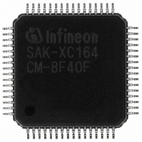
SAK-XC164CM-8F40F AA Infineon Technologies, SAK-XC164CM-8F40F AA Datasheet - Page 13

SAK-XC164CM-8F40F AA
Manufacturer Part Number
SAK-XC164CM-8F40F AA
Description
IC MCU 16BIT 64KB FLSH TQFP-64-8
Manufacturer
Infineon Technologies
Series
XC16xr
Datasheet
1.SAF-XC164CM-4F20F_AA.pdf
(70 pages)
Specifications of SAK-XC164CM-8F40F AA
Core Processor
C166SV2
Core Size
16-Bit
Speed
40MHz
Connectivity
CAN, SPI, UART/USART
Peripherals
PWM, WDT
Number Of I /o
47
Program Memory Size
64KB (64K x 8)
Program Memory Type
FLASH
Ram Size
6K x 8
Voltage - Supply (vcc/vdd)
2.35 V ~ 2.7 V
Data Converters
A/D 14x8/10b
Oscillator Type
Internal
Operating Temperature
-40°C ~ 125°C
Package / Case
64-LFQFP
Data Bus Width
16 bit
Data Ram Size
6 KB
Interface Type
2xASC, 2xSSC
Maximum Clock Frequency
40 MHz
Number Of Programmable I/os
47
Number Of Timers
9
Operating Supply Voltage
5 V
Maximum Operating Temperature
+ 125 C
Mounting Style
SMD/SMT
Minimum Operating Temperature
- 40 C
On-chip Adc
10 bit, 14 Channel
Packages
PG-LQFP-64
Max Clock Frequency
40.0 MHz
Sram (incl. Cache)
6.0 KByte
Can Nodes
2
A / D Input Lines (incl. Fadc)
14
Program Memory
64.0 KByte
For Use With
B158-H8961-X-X-7600IN - KIT EASY XC164CMXC164CMUCANIN - KIT U-CAN STARTER XC164CMMCBX167-NET - BOARD EVAL INFINEON CAN/ETHRNTMCBXC167-BASIC - BOARD EVAL BASIC INFINEON XC16X
Lead Free Status / RoHS Status
Lead free / RoHS Compliant
Eeprom Size
-
Lead Free Status / Rohs Status
Details
Other names
SAK-XC164CM-8F40FAACT
SAK-XC164CM-8F40FAACT
SAK-XC164CM-8F40FAAINCT
SAK-XC164CM-8F40FAACT
SAK-XC164CM-8F40FAAINCT
Table 2
Sym-
bol
Port 3
P3.1
P3.2
P3.3
P3.4
P3.5
P3.6
P3.7
P3.8
P3.9
P3.10
P3.11
P3.13
P3.15
Data Sheet
Pin
Num.
28-39,
42
28
29
30
31
32
33
34
35
36
37
38
39
42
Pin Definitions and Functions (cont’d)
Input
Outp.
IO
O
I/O
I
I
I
I
O
O
I
I
I
O
O
I
I
I
I/O
I/O
O
I
I/O
I
I/O
I
O
O
Function
Port 3 is a 13-bit bidirectional I/O port. Each pin can be
programmed for input (output driver in high-impedance state)
or output (configurable as push/pull or open drain driver). The
input threshold of Port 3 is selectable (standard or
special).The following Port 3 pins also serve for alternate
functions:
T6OUT: [GPT2] Timer T6 Toggle Latch Output,
RxD1: [ASC1] Data Input (Async.) or Inp./Outp. (Sync.),
EX1IN: [Fast External Interrupt 1] Input (alternate pin A),
TCK: [Debug System] JTAG Clock Input
CAPIN: [GPT2] Register CAPREL Capture Input,
TDI: [Debug System] JTAG Data In
T3OUT: [GPT1] Timer T3 Toggle Latch Output,
TDO: [Debug System] JTAG Data Out
T3EUD: [GPT1] Timer T3 External Up/Down Control Input,
TMS: [Debug System] JTAG Test Mode Selection
T4IN: [GPT1] Timer T4 Count/Gate/Reload/Capture Inp.
TxD1: [ASC0] Clock/Data Output (Async./Sync.),
BRKOUT: [Debug System] Break Out
T3IN: [GPT1] Timer T3 Count/Gate Input
T2IN: [GPT1] Timer T2 Count/Gate/Reload/Capture Inp.
BRKIN: [Debug System] Break In
MRST0: [SSC0] Master-Receive/Slave-Transmit In/Out.
MTSR0: [SSC0] Master-Transmit/Slave-Receive Out/In.
TxD0: [ASC0] Clock/Data Output (Async./Sync.),
EX2IN: [Fast External Interrupt 2] Input (alternate pin B)
RxD0: [ASC0] Data Input (Async.) or Inp./Outp. (Sync.),
EX2IN: [Fast External Interrupt 2] Input (alternate pin A)
SCLK0: [SSC0] Master Clock Output / Slave Clock Input.,
EX3IN: [Fast External Interrupt 3] Input (alternate pin A)
CLKOUT: System Clock Output (= CPU Clock),
FOUT: Programmable Frequency Output
11
General Device Information
Derivatives
V1.4, 2007-03
XC164CM


