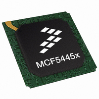
MCF54452VR266 Freescale Semiconductor, MCF54452VR266 Datasheet - Page 25

MCF54452VR266
Manufacturer Part Number
MCF54452VR266
Description
IC MPU 32BIT 266MHZ 360TEPBGA
Manufacturer
Freescale Semiconductor
Series
MCF5445xr
Datasheet
1.MCF54452CVR200.pdf
(48 pages)
Specifications of MCF54452VR266
Core Processor
Coldfire V4
Core Size
32-Bit
Speed
266MHz
Connectivity
I²C, SPI, SSI, UART/USART, USB OTG
Peripherals
DMA, WDT
Number Of I /o
132
Program Memory Type
ROMless
Ram Size
32K x 8
Voltage - Supply (vcc/vdd)
1.35 V ~ 3.6 V
Oscillator Type
Internal
Operating Temperature
0°C ~ 70°C
Package / Case
360-TEPBGA
Family Name
MCF5445X
Device Core
ColdFire
Device Core Size
32b
Frequency (max)
266MHz
Instruction Set Architecture
RISC
Supply Voltage 1 (typ)
3.3V
Operating Supply Voltage (max)
1.65/3.6V
Operating Supply Voltage (min)
1.35/3V
Operating Temp Range
0C to 70C
Operating Temperature Classification
Commercial
Mounting
Surface Mount
Pin Count
360
Package Type
TEBGA
Leaded Process Compatible
Yes
Rohs Compliant
Yes
Peak Reflow Compatible (260 C)
Yes
For Use With
M54455EVB - BOARD EVAL FOR MCF5445X
Lead Free Status / RoHS Status
Lead free / RoHS Compliant
Eeprom Size
-
Program Memory Size
-
Data Converters
-
Lead Free Status / Rohs Status
Compliant
Available stocks
Company
Part Number
Manufacturer
Quantity
Price
Company:
Part Number:
MCF54452VR266
Manufacturer:
Freescale Semiconductor
Quantity:
135
Company:
Part Number:
MCF54452VR266
Manufacturer:
FREESCAL
Quantity:
329
1
2
3
4
5
6
7
8
DD10 Input Data Hold Relative to DQS.
Num
DD1
DD2
DD3
DD4
DD5
DD6
DD7
DD8
DD9
5.8
The following timing numbers must be followed to properly latch or drive data onto the SDRAM memory bus. All timing
numbers are relative to the four DQS byte lanes.
Freescale Semiconductor
The SDRAM interface operates at the same frequency as the internal system bus.
Pulse width high plus pulse width low cannot exceed min and max clock period.
Command output valid should be 1/2 the memory bus clock (t
voltage variations.
This specification relates to the required input setup time of DDR memories. The microprocessor’s output setup should be larger
than the input setup of the DDR memories. If it is not larger, then the input setup on the memory is in violation.
SD_D[31:24] is relative to SD_DQS[3]; SD_D[23:16] is relative to SD_DQS[2]
The first data beat is valid before the first rising edge of DQS and after the DQS write preamble. The remaining data beats are valid
for each subsequent DQS edge.
This specification relates to the required hold time of DDR memories.
SD_D[31:24] is relative to SD_DQS[3]; SD_D[23:16] is relative to SD_DQS[2]
Data input skew is derived from each DQS clock edge. It begins with a DQS transition and ends when the last data line becomes
Data input hold is derived from each DQS clock edge. It begins with a DQS transition and ends when the first data line becomes
invalid.
valid. This input skew must include DDR memory output skew and system level board skew (due to routing or other factors).
Frequency of Operation
Clock Period
Pulse Width High
Pulse Width Low
Address, SD_CKE, SD_CAS, SD_RAS, SD_WE,
SD_CS[1:0] — Output Valid
Address, SD_CKE, SD_CAS, SD_RAS, SD_WE,
SD_CS[1:0] — Output Hold
Write Command to first DQS Latching Transition
Data and Data Mask Output Setup (DQ-->DQS)
Relative to DQS (DDR Write Mode)
Data and Data Mask Output Hold (DQS-->DQ)
Relative to DQS (DDR Write Mode)
Input Data Skew Relative to DQS (Input Setup)
SDRAM AC Timing Characteristics
Characteristic
MCF5445x ColdFire
Table 13. SDRAM Timing Specifications
®
Microprocessor Data Sheet, Rev. 6
SDCK
Symbol
t
t
t
t
SDCKH
SDCKL
t
t
SDCK
DQSS
CMV
CMH
t
t
t
t
QS
QH
IS
IH
) plus some minor adjustments for process, temperature, and
(0.25 x t
(1.0 x t
+ 0.5ns
- 0.6ns
0.45
0.45
Min
7.5
2.0
1.0
1.0
60
—
—
SDCK
SDCK
)
)
(0.5 x t
(1.0 x t
+ 1.0ns
+ 0.6ns
133.33
16.67
Max
0.55
0.55
1.0
—
—
—
—
Electrical Characteristics
SDCK
SDCK
)
)
t
t
Unit
MHz
SDCK
SDCK
ns
ns
ns
ns
ns
ns
ns
ns
Notes
3
25
1
2
3
4
5
6
7
8


