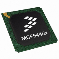
MCF54452VR266 Freescale Semiconductor, MCF54452VR266 Datasheet - Page 17

MCF54452VR266
Manufacturer Part Number
MCF54452VR266
Description
IC MPU 32BIT 266MHZ 360TEPBGA
Manufacturer
Freescale Semiconductor
Series
MCF5445xr
Datasheet
1.MCF54452CVR200.pdf
(48 pages)
Specifications of MCF54452VR266
Core Processor
Coldfire V4
Core Size
32-Bit
Speed
266MHz
Connectivity
I²C, SPI, SSI, UART/USART, USB OTG
Peripherals
DMA, WDT
Number Of I /o
132
Program Memory Type
ROMless
Ram Size
32K x 8
Voltage - Supply (vcc/vdd)
1.35 V ~ 3.6 V
Oscillator Type
Internal
Operating Temperature
0°C ~ 70°C
Package / Case
360-TEPBGA
Family Name
MCF5445X
Device Core
ColdFire
Device Core Size
32b
Frequency (max)
266MHz
Instruction Set Architecture
RISC
Supply Voltage 1 (typ)
3.3V
Operating Supply Voltage (max)
1.65/3.6V
Operating Supply Voltage (min)
1.35/3V
Operating Temp Range
0C to 70C
Operating Temperature Classification
Commercial
Mounting
Surface Mount
Pin Count
360
Package Type
TEBGA
Leaded Process Compatible
Yes
Rohs Compliant
Yes
Peak Reflow Compatible (260 C)
Yes
For Use With
M54455EVB - BOARD EVAL FOR MCF5445X
Lead Free Status / RoHS Status
Lead free / RoHS Compliant
Eeprom Size
-
Program Memory Size
-
Data Converters
-
Lead Free Status / Rohs Status
Compliant
Available stocks
Company
Part Number
Manufacturer
Quantity
Price
Company:
Part Number:
MCF54452VR266
Manufacturer:
Freescale Semiconductor
Quantity:
135
Company:
Part Number:
MCF54452VR266
Manufacturer:
FREESCAL
Quantity:
329
5
This document contains electrical specification tables and reference timing diagrams for the MCF54455 microprocessor. This
section contains detailed information on DC/AC electrical characteristics and AC timing specifications.
The electrical specifications are preliminary and from previous designs or design simulations. These specifications may not be
fully tested or guaranteed at this early stage of the product life cycle. However, for production silicon, these specifications will
be met. Finalized specifications will be published after complete characterization and device qualifications have been
completed.
5.1
Freescale Semiconductor
1
2
3
4
5
External I/O pad supply voltage
Internal oscillator supply voltage
Real-time clock supply voltage
Internal logic supply voltage
SDRAM I/O pad supply voltage
PLL supply voltage
Digital input voltage
Instantaneous maximum current
Single pin limit (applies to all pins)
Operating temperature range (packaged)
Storage temperature range
Functional operating conditions are given in
operation at the maximum is not guaranteed. Continued operation at these levels may affect device reliability or cause
permanent damage to the device.
This device contains circuitry protecting against damage due to high static voltage or electrical fields. However, it is
advised that normal precautions be taken to avoid application of any voltages higher than maximum-rated voltages to this
high-impedance circuit. Reliability of operation is enhanced if unused inputs are tied to an appropriate logic voltage level
(e.g., V
Input must be current limited to the value specified. To determine the value of the required current-limiting resistor,
calculate resistance values for positive and negative clamp voltages, and then use the larger of the two values.
All functional non-supply pins are internally clamped to V
Power supply must maintain regulation within operating EV
current conditions. If positive injection current (V
and could result in external power supply going out of regulation. Ensure the external EV
than maximum injection current. This is the greatest risk when the MPU is not consuming power (ex; no clock). The power
supply must maintain regulation within operating EV
conditions.
Electrical Characteristics
Absolute Maximum Ratings
SS
or EV
The parameters specified in this MCU document supersede any values found in the module
specifications.
DD
3
).
Rating
MCF5445x ColdFire
3, 4, 5
Table 5. Absolute Maximum Ratings
Table
in
®
> EV
8.
Microprocessor Data Sheet, Rev. 6
DD
Absolute maximum ratings are stress ratings only, and functional
NOTE
DD
range during instantaneous and operating maximum current
SS
) is greater than I
OSCV
RTCV
(T
Symbol
DD
SDV
and EV
EV
PV
IV
L
T
V
I
T
DD
range during instantaneous and operating maximum
- T
stg
DD
IN
A
DD
DD
DD
DD
DD
H
)
DD
.
VDD_A_PLL
VDD_OSC
VDD_RTC
Pin Name
SD_VDD
EVDD
IVDD
DD
—
—
—
—
, the injection current may flow out of EV
1, 2
DD
-0.3 to +4.0
-0.3 to +4.0
-0.5 to +2.0
-0.5 to +2.0
-0.3 to +4.0
-0.5 to +2.0
-0.3 to +3.6
-55 to +150
-40 to +85
load shunts current greater
Value
25
Electrical Characteristics
Units
mA
°C
°C
V
V
V
V
V
V
V
DD
17


