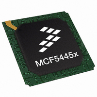
MCF54452VR266 Freescale Semiconductor, MCF54452VR266 Datasheet - Page 19

MCF54452VR266
Manufacturer Part Number
MCF54452VR266
Description
IC MPU 32BIT 266MHZ 360TEPBGA
Manufacturer
Freescale Semiconductor
Series
MCF5445xr
Datasheet
1.MCF54452CVR200.pdf
(48 pages)
Specifications of MCF54452VR266
Core Processor
Coldfire V4
Core Size
32-Bit
Speed
266MHz
Connectivity
I²C, SPI, SSI, UART/USART, USB OTG
Peripherals
DMA, WDT
Number Of I /o
132
Program Memory Type
ROMless
Ram Size
32K x 8
Voltage - Supply (vcc/vdd)
1.35 V ~ 3.6 V
Oscillator Type
Internal
Operating Temperature
0°C ~ 70°C
Package / Case
360-TEPBGA
Family Name
MCF5445X
Device Core
ColdFire
Device Core Size
32b
Frequency (max)
266MHz
Instruction Set Architecture
RISC
Supply Voltage 1 (typ)
3.3V
Operating Supply Voltage (max)
1.65/3.6V
Operating Supply Voltage (min)
1.35/3V
Operating Temp Range
0C to 70C
Operating Temperature Classification
Commercial
Mounting
Surface Mount
Pin Count
360
Package Type
TEBGA
Leaded Process Compatible
Yes
Rohs Compliant
Yes
Peak Reflow Compatible (260 C)
Yes
For Use With
M54455EVB - BOARD EVAL FOR MCF5445X
Lead Free Status / RoHS Status
Lead free / RoHS Compliant
Eeprom Size
-
Program Memory Size
-
Data Converters
-
Lead Free Status / Rohs Status
Compliant
Available stocks
Company
Part Number
Manufacturer
Quantity
Price
Company:
Part Number:
MCF54452VR266
Manufacturer:
Freescale Semiconductor
Quantity:
135
Company:
Part Number:
MCF54452VR266
Manufacturer:
FREESCAL
Quantity:
329
where K is a constant pertaining to the particular part. K can be determined from
for a known T
for any value of T
5.3
5.4
Freescale Semiconductor
Internal logic supply voltage
PLL analog operation voltage range
External I/O pad supply voltage
Internal oscillator supply voltage
Real-time clock supply voltage
SDRAM I/O pad supply voltage — DDR mode
SDRAM I/O pad supply voltage — DDR2 mode
SDRAM I/O pad supply voltage — Mobile DDR mode
SDRAM input reference voltage
Input High Voltage
Input Low Voltage
Input Hysteresis
Input Leakage Current
High Impedance (Off-State) Leakage Current
Output High Voltage (All input/output and all output pins)
Output Low Voltage (All input/output and all output pins)
V
V
I
I
OH
OL
in
in
= V
= V
= 5.0mA
= –5.0 mA
ESD Protection
DC Electrical Specifications
DD
DD
A
. Using this value of K, the values of P
or V
or V
1
2
A
ESD Target for Human Body Model
.
All ESD testing is in conformity with CDF-AEC-Q100 Stress Test Qualification for
Automotive Grade Integrated Circuits.
A device is defined as a failure if after exposure to ESD pulses the device no longer meets
the device specification requirements. Complete DC parametric and functional testing is
performed per applicable device specification at room temperature followed by hot
temperature, unless specified otherwise in the device specification.
SS
SS
, All input/output and output pins
, Input-only pins
Characteristics
Characteristic
1
MCF5445x ColdFire
Table 7. ESD Protection Characteristics
1
Table 8. DC Electrical Specifications
2
D
®
and T
Microprocessor Data Sheet, Rev. 6
J
Symbol
can be obtained by solving
HBM
OSCV
RTCV
Symbol
SDV
SDV
SDV
SDV
PV
EV
V
IV
V
V
V
I
V
HYS
I
OZ
Value
OH
OL
in
2000
DD
IH
IL
DD
DD
REF
DD
DD
DD
Equation 3
DD
DD
1, 2
0.49 x SDV
0.06 x EV
0.85 × EV
0.7 x EV
Equation 1
V
SS
–10.0
1.35
1.35
1.35
2.25
–2.5
Min
3.0
3.0
1.7
1.7
by measuring P
__
– 0.3
Units
DD
DD
DD
DD
V
Electrical Characteristics
and
0.51 x SDV
0.35 x EV
0.15 × EV
Equation 2
Max
1.65
1.65
1.65
2.75
3.65
10.0
3.6
3.6
1.9
1.9
2.5
__
—
D
(at equilibrium)
DD
DD
DD
iteratively
Units
mV
μA
μA
V
V
V
V
V
V
V
V
V
V
V
V
V
19


