C8051F530-IT Silicon Laboratories Inc, C8051F530-IT Datasheet - Page 62
C8051F530-IT
Manufacturer Part Number
C8051F530-IT
Description
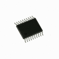
IC 8051 MCU 8K FLASH 20TSSOP
Manufacturer
Silicon Laboratories Inc
Series
C8051F53xr
Datasheet
1.C8051F530-TB.pdf
(218 pages)
Specifications of C8051F530-IT
Core Processor
8051
Core Size
8-Bit
Speed
25MHz
Connectivity
LIN, SPI, UART/USART
Peripherals
Brown-out Detect/Reset, POR, PWM, Temp Sensor, WDT
Number Of I /o
16
Program Memory Size
8KB (8K x 8)
Program Memory Type
FLASH
Ram Size
256 x 8
Voltage - Supply (vcc/vdd)
2 V ~ 5.25 V
Data Converters
A/D 16x12b
Oscillator Type
Internal
Operating Temperature
-40°C ~ 125°C
Package / Case
20-TSSOP
Lead Free Status / RoHS Status
Lead free / RoHS Compliant
Eeprom Size
-
Other names
336-1343
Available stocks
Company
Part Number
Manufacturer
Quantity
Price
Company:

Part Number:
C8051F530-IT
Manufacturer:
SILICON
Quantity:
195


C8051F52x/F52xA/F53x/F53xA
For example, the initial example in this section requires a gain of 0.44 to convert 5 V full scale to 2.2 V full
scale. Using Equation 4.3:
If GAINADD is set to 1, this makes the equation:
The actual gain from setting GAINADD to 1 and ADC0GNH and ADC0GNL to 0x6CA is 0.4399. A similar
gain can be achieved if GAINADD is set to 0 with a different value for ADC0GNH and ADC0GNL.
4.4.2. Setting the Gain Value
The three programmable gain registers are accessed indirectly using the ADC0H and ADC0L registers
when the GAINEN bit (ADC0CF.0) bit is set. ADC0H acts as the address register, and ADC0L is the data
register. The programmable gain registers can only be written to and cannot be read. See Gain Register
Definition 4.1, Gain Register Definition 4.2, and Gain Register Definition 4.3 for more information.
The gain is programmed using the following steps:
1. Set the GAINEN bit (ADC0CF.0)
2. Load the ADC0H with the ADC0GNH, ADC0GNL, or ADC0GNA address.
3. Load ADC0L with the desired value for the selected gain register.
4. Reset the GAINEN bit (ADC0CF.0)
Notes:
In code, changing the value to 0.44 gain from the previous example looks like:
// in ‘C’:
ADC0CF |= 0x01;// GAINEN = 1
ADC0H = 0x04;// Load the ADC0GNH address
ADC0L = 0x6C;// Load the upper byte of 0x6CA to ADC0GNH
ADC0H = 0x07;// Load the ADC0GNL address
ADC0L = 0xA0;// Load the lower nibble of 0x6CA to ADC0GNL
ADC0H = 0x08;// Load the ADC0GNA address
ADC0L = 0x01;// Set the GAINADD bit
ADC0CF &= ~0x01;// GAINEN = 0
; in assembly
ORL ADC0CF,#01H ; GAINEN = 1
MOV ADC0H,#04H; Load the ADC0GNH address
MOV ADC0L,#06CH ; Load the upper byte of 0x6CA to ADC0GNH
MOV ADC0H,#07H; Load the ADC0GNL address
MOV ADC0L,#0A0H ; Load the lower nibble of 0x6CA to ADC0GNL
MOV ADC0H,#08H; Load the ADC0GNA address
MOV ADC0L,#01H ; Set the GAINADD bit
ANL ADC0CF,#0FEH ; GAINEN = 0
62
1. An ADC conversion should not be performed while the GAINEN bit is set.
2.
Even with gain enabled, the maximum input voltage must be less than V
voltage of the signal after gain must be less than or equal to V
GAIN
=
0.44 1
GAIN
–
=
----- -
64
1
0.44 GAINADD
–
4096
Rev. 1.3
=
0.424 4096
----- -
64
1
REF
=
4096
.
1738
REGIN
=
0x06CA
and the maximum
Related parts for C8051F530-IT
Image
Part Number
Description
Manufacturer
Datasheet
Request
R

Part Number:
Description:
SMD/C°/SINGLE-ENDED OUTPUT SILICON OSCILLATOR
Manufacturer:
Silicon Laboratories Inc
Part Number:
Description:
Manufacturer:
Silicon Laboratories Inc
Datasheet:
Part Number:
Description:
N/A N/A/SI4010 AES KEYFOB DEMO WITH LCD RX
Manufacturer:
Silicon Laboratories Inc
Datasheet:
Part Number:
Description:
N/A N/A/SI4010 SIMPLIFIED KEY FOB DEMO WITH LED RX
Manufacturer:
Silicon Laboratories Inc
Datasheet:
Part Number:
Description:
N/A/-40 TO 85 OC/EZLINK MODULE; F930/4432 HIGH BAND (REV E/B1)
Manufacturer:
Silicon Laboratories Inc
Part Number:
Description:
EZLink Module; F930/4432 Low Band (rev e/B1)
Manufacturer:
Silicon Laboratories Inc
Part Number:
Description:
I°/4460 10 DBM RADIO TEST CARD 434 MHZ
Manufacturer:
Silicon Laboratories Inc
Part Number:
Description:
I°/4461 14 DBM RADIO TEST CARD 868 MHZ
Manufacturer:
Silicon Laboratories Inc
Part Number:
Description:
I°/4463 20 DBM RFSWITCH RADIO TEST CARD 460 MHZ
Manufacturer:
Silicon Laboratories Inc
Part Number:
Description:
I°/4463 20 DBM RADIO TEST CARD 868 MHZ
Manufacturer:
Silicon Laboratories Inc
Part Number:
Description:
I°/4463 27 DBM RADIO TEST CARD 868 MHZ
Manufacturer:
Silicon Laboratories Inc
Part Number:
Description:
I°/4463 SKYWORKS 30 DBM RADIO TEST CARD 915 MHZ
Manufacturer:
Silicon Laboratories Inc
Part Number:
Description:
N/A N/A/-40 TO 85 OC/4463 RFMD 30 DBM RADIO TEST CARD 915 MHZ
Manufacturer:
Silicon Laboratories Inc
Part Number:
Description:
I°/4463 20 DBM RADIO TEST CARD 169 MHZ
Manufacturer:
Silicon Laboratories Inc