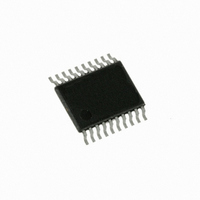
C8051F530-IT Silicon Laboratories Inc, C8051F530-IT Datasheet - Page 22

C8051F530-IT
Manufacturer Part Number
C8051F530-IT
Description
IC 8051 MCU 8K FLASH 20TSSOP
Manufacturer
Silicon Laboratories Inc
Series
C8051F53xr
Datasheet
1.C8051F530-TB.pdf
(218 pages)
Specifications of C8051F530-IT
Core Processor
8051
Core Size
8-Bit
Speed
25MHz
Connectivity
LIN, SPI, UART/USART
Peripherals
Brown-out Detect/Reset, POR, PWM, Temp Sensor, WDT
Number Of I /o
16
Program Memory Size
8KB (8K x 8)
Program Memory Type
FLASH
Ram Size
256 x 8
Voltage - Supply (vcc/vdd)
2 V ~ 5.25 V
Data Converters
A/D 16x12b
Oscillator Type
Internal
Operating Temperature
-40°C ~ 125°C
Package / Case
20-TSSOP
Lead Free Status / RoHS Status
Lead free / RoHS Compliant
Eeprom Size
-
Other names
336-1343
Available stocks
Company
Part Number
Manufacturer
Quantity
Price
Company:
Part Number:
C8051F530-IT
Manufacturer:
SILICON
Quantity:
195
- Current page: 22 of 218
- Download datasheet (2Mb)
C8051F52x/F52xA/F53x/F53xA
1.5. 12-Bit Analog to Digital Converter
The C8051F52x/F52xA/F53x/F53xA devices include an on-chip 12-bit SAR ADC with a maximum through-
put of 200 ksps. The ADC system includes a configurable analog multiplexer that selects the positive ADC
input, which is measured with respect to GND. Ports 0 and 1 are available as ADC inputs; additionally, the
ADC includes an innovative programmable gain stage which allows the ADC to sample inputs sources
greater than the VREF voltage. The on-chip Temperature Sensor output and the core supply voltage (V
are also available as ADC inputs. User firmware may shut down the ADC or use it in Burst Mode to save
power.
Conversions can be initiated in four ways: a software command, an overflow of Timer 1, an overflow of
Timer 2, or an external convert start signal. This flexibility allows the start of conversion to be triggered by
software events, a periodic signal (timer overflows), or external HW signals. Conversion completions are
indicated by a status bit and an interrupt (if enabled) and occur after 1, 4, 8, or 16 samples have been
accumulated by a hardware accumulator. The resulting 12-bit to 16-bit data word is latched into the ADC
data SFRs upon completion of a conversion. When the system clock is slow, Burst Mode allows ADC0 to
automatically wake from a low power shutdown state, acquire and accumulate samples, then re-enter the
low power shutdown state without CPU intervention.
Window compare registers for the ADC data can be configured to interrupt the controller when ADC data is
either within or outside of a specified range. The ADC can monitor a key voltage continuously in back-
ground mode, but not interrupt the controller unless the converted data is within/outside the specified
range.
1.6. Programmable Comparator
C8051F52x/F52xA/F53x/F53xA devices include a software-configurable voltage comparator with an input
multiplexer. The comparator offers programmable response time and hysteresis and an output that is
optionally available at the Port pins: a synchronous “latched” output (CP0). The comparator interrupt may
be generated on rising, falling, or both edges. When in IDLE or SUSPEND mode, these interrupts may be
used as a “wake-up” source for the processor. The Comparator may also be configured as a reset source.
A block diagram of the comparator is shown in Figure 1.8.
22
Sensor
Temp
Analog Multiplexer
* Available on ‘F53x/
P0.6*
P0.7*
P1.0*
P1.7*
’F53xA devices
GND
VDD
P0.0
19-to-1
AMUX
Figure 1.7. 12-Bit ADC Block Diagram
Selectable
Gain
Configuration, Control, and Data Registers
Burst Mode
Logic
Rev. 1.3
ADC
12-Bit
SAR
End of
Conversion
Interrupt
Conversion
Start
16
Window Compare
Logic
Accumulator
AD0BUSY (W)
Timer 1 Overflow
CNVSTR Rising Edge
Timer 2 Overflow
ADC Data
Registers
Window
Compare
Interrupt
DD
)
Related parts for C8051F530-IT
Image
Part Number
Description
Manufacturer
Datasheet
Request
R
Part Number:
Description:
SMD/C°/SINGLE-ENDED OUTPUT SILICON OSCILLATOR
Manufacturer:
Silicon Laboratories Inc
Part Number:
Description:
Manufacturer:
Silicon Laboratories Inc
Datasheet:
Part Number:
Description:
N/A N/A/SI4010 AES KEYFOB DEMO WITH LCD RX
Manufacturer:
Silicon Laboratories Inc
Datasheet:
Part Number:
Description:
N/A N/A/SI4010 SIMPLIFIED KEY FOB DEMO WITH LED RX
Manufacturer:
Silicon Laboratories Inc
Datasheet:
Part Number:
Description:
N/A/-40 TO 85 OC/EZLINK MODULE; F930/4432 HIGH BAND (REV E/B1)
Manufacturer:
Silicon Laboratories Inc
Part Number:
Description:
EZLink Module; F930/4432 Low Band (rev e/B1)
Manufacturer:
Silicon Laboratories Inc
Part Number:
Description:
I°/4460 10 DBM RADIO TEST CARD 434 MHZ
Manufacturer:
Silicon Laboratories Inc
Part Number:
Description:
I°/4461 14 DBM RADIO TEST CARD 868 MHZ
Manufacturer:
Silicon Laboratories Inc
Part Number:
Description:
I°/4463 20 DBM RFSWITCH RADIO TEST CARD 460 MHZ
Manufacturer:
Silicon Laboratories Inc
Part Number:
Description:
I°/4463 20 DBM RADIO TEST CARD 868 MHZ
Manufacturer:
Silicon Laboratories Inc
Part Number:
Description:
I°/4463 27 DBM RADIO TEST CARD 868 MHZ
Manufacturer:
Silicon Laboratories Inc
Part Number:
Description:
I°/4463 SKYWORKS 30 DBM RADIO TEST CARD 915 MHZ
Manufacturer:
Silicon Laboratories Inc
Part Number:
Description:
N/A N/A/-40 TO 85 OC/4463 RFMD 30 DBM RADIO TEST CARD 915 MHZ
Manufacturer:
Silicon Laboratories Inc
Part Number:
Description:
I°/4463 20 DBM RADIO TEST CARD 169 MHZ
Manufacturer:
Silicon Laboratories Inc


