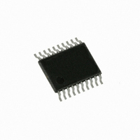
C8051F530-IT Silicon Laboratories Inc, C8051F530-IT Datasheet - Page 163

C8051F530-IT
Manufacturer Part Number
C8051F530-IT
Description
IC 8051 MCU 8K FLASH 20TSSOP
Manufacturer
Silicon Laboratories Inc
Series
C8051F53xr
Datasheet
1.C8051F530-TB.pdf
(218 pages)
Specifications of C8051F530-IT
Core Processor
8051
Core Size
8-Bit
Speed
25MHz
Connectivity
LIN, SPI, UART/USART
Peripherals
Brown-out Detect/Reset, POR, PWM, Temp Sensor, WDT
Number Of I /o
16
Program Memory Size
8KB (8K x 8)
Program Memory Type
FLASH
Ram Size
256 x 8
Voltage - Supply (vcc/vdd)
2 V ~ 5.25 V
Data Converters
A/D 16x12b
Oscillator Type
Internal
Operating Temperature
-40°C ~ 125°C
Package / Case
20-TSSOP
Lead Free Status / RoHS Status
Lead free / RoHS Compliant
Eeprom Size
-
Other names
336-1343
Available stocks
Company
Part Number
Manufacturer
Quantity
Price
Company:
Part Number:
C8051F530-IT
Manufacturer:
SILICON
Quantity:
195
- Current page: 163 of 218
- Download datasheet (2Mb)
17. LIN (C8051F520/0A/3/3A/6/6A and C8051F530/0A/3/3A/6/6A)
Important Note: This chapter assumes an understanding of the Local Interconnect Network (LIN) proto-
col. For more information about the LIN protocol, including specifications, please refer to the LIN consor-
tium (http://www.lin-subbus.org/).
LIN is an asynchronous, serial communications interface used primarily in automotive networks. The Sili-
con Laboratories LIN controller is compliant to the 2.1 Specification, implements a complete hardware LIN
interface, and includes the following features:
Note: The minimum system clock (SYSCLK) required when using the LIN peripheral is 8 MHz.
The LIN peripheral has four main components:
Selectable Master and Slave modes.
Automatic baud rate option in slave mode
The internal oscillator is accurate to within 0.5% of 24.5 MHz across the entire temperature range and
for VDD voltages greater than or equal to the minimum output of the on-chip voltage regulator, so an
external oscillator is not necessary for master mode operation for most systems.
1. LIN Access Registers—Provide the interface between the MCU core and the LIN peripheral.
2. LIN Data Registers—Where transmitted and received message data bytes are stored.
3. LIN Control Registers—Control the functionality of the LIN interface.
4. Control State Machine and Bit Streaming Logic—Contains the hardware that serializes mes-
sages and controls the bus timing of the controller.
RX
TX
Indirectly Addressed Registers
Registers
LIN Data
Control State Machine
LIN Controller
Figure 17.1. LIN Block Diagram
C8051F520/0A/3/3A/6/6A and C8051F530/0A/3/3A/6/6A
C8051F52x/F52xA/F53x/F53xA
LIN Control
Registers
Rev. 1.3
8051 MCU Core
LINADDR
LINDATA
LINCF
163
Related parts for C8051F530-IT
Image
Part Number
Description
Manufacturer
Datasheet
Request
R
Part Number:
Description:
SMD/C°/SINGLE-ENDED OUTPUT SILICON OSCILLATOR
Manufacturer:
Silicon Laboratories Inc
Part Number:
Description:
Manufacturer:
Silicon Laboratories Inc
Datasheet:
Part Number:
Description:
N/A N/A/SI4010 AES KEYFOB DEMO WITH LCD RX
Manufacturer:
Silicon Laboratories Inc
Datasheet:
Part Number:
Description:
N/A N/A/SI4010 SIMPLIFIED KEY FOB DEMO WITH LED RX
Manufacturer:
Silicon Laboratories Inc
Datasheet:
Part Number:
Description:
N/A/-40 TO 85 OC/EZLINK MODULE; F930/4432 HIGH BAND (REV E/B1)
Manufacturer:
Silicon Laboratories Inc
Part Number:
Description:
EZLink Module; F930/4432 Low Band (rev e/B1)
Manufacturer:
Silicon Laboratories Inc
Part Number:
Description:
I°/4460 10 DBM RADIO TEST CARD 434 MHZ
Manufacturer:
Silicon Laboratories Inc
Part Number:
Description:
I°/4461 14 DBM RADIO TEST CARD 868 MHZ
Manufacturer:
Silicon Laboratories Inc
Part Number:
Description:
I°/4463 20 DBM RFSWITCH RADIO TEST CARD 460 MHZ
Manufacturer:
Silicon Laboratories Inc
Part Number:
Description:
I°/4463 20 DBM RADIO TEST CARD 868 MHZ
Manufacturer:
Silicon Laboratories Inc
Part Number:
Description:
I°/4463 27 DBM RADIO TEST CARD 868 MHZ
Manufacturer:
Silicon Laboratories Inc
Part Number:
Description:
I°/4463 SKYWORKS 30 DBM RADIO TEST CARD 915 MHZ
Manufacturer:
Silicon Laboratories Inc
Part Number:
Description:
N/A N/A/-40 TO 85 OC/4463 RFMD 30 DBM RADIO TEST CARD 915 MHZ
Manufacturer:
Silicon Laboratories Inc
Part Number:
Description:
I°/4463 20 DBM RADIO TEST CARD 169 MHZ
Manufacturer:
Silicon Laboratories Inc


