MC68HC908EY16CFA Freescale Semiconductor, MC68HC908EY16CFA Datasheet - Page 24
MC68HC908EY16CFA
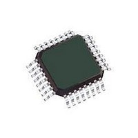
Manufacturer Part Number
MC68HC908EY16CFA
Description
IC MCU 16K FLASH 8MHZ SPI 32LQFP
Manufacturer
Freescale Semiconductor
Series
HC08r
Datasheet
1.MC908EY16VFAR2.pdf
(278 pages)
Specifications of MC68HC908EY16CFA
Core Processor
HC08
Core Size
8-Bit
Speed
8MHz
Connectivity
LIN, SCI, SPI
Peripherals
POR, PWM
Number Of I /o
24
Program Memory Size
16KB (16K x 8)
Program Memory Type
FLASH
Ram Size
512 x 8
Voltage - Supply (vcc/vdd)
4.5 V ~ 5.5 V
Data Converters
A/D 8x10b
Oscillator Type
Internal
Operating Temperature
-40°C ~ 85°C
Package / Case
32-LQFP
Processor Series
HC08EY
Core
HC08
Data Bus Width
8 bit
Data Ram Size
512 B
Interface Type
ESCI, SPI
Maximum Clock Frequency
8 MHz
Number Of Programmable I/os
24
Number Of Timers
4
Maximum Operating Temperature
+ 85 C
Mounting Style
SMD/SMT
Development Tools By Supplier
FSICEBASE, M68CBL05CE, ZK-HC08EY-A
Minimum Operating Temperature
- 40 C
On-chip Adc
10 bit, 8 Channel
Lead Free Status / RoHS Status
Contains lead / RoHS non-compliant
Eeprom Size
-
Lead Free Status / Rohs Status
No
Available stocks
Company
Part Number
Manufacturer
Quantity
Price
Company:

Part Number:
MC68HC908EY16CFA
Manufacturer:
FREESCALE
Quantity:
1 831
Company:
Part Number:
MC68HC908EY16CFA
Manufacturer:
QFP
Quantity:
453
Company:
Part Number:
MC68HC908EY16CFA
Manufacturer:
Freescale Semiconductor
Quantity:
10 000


General Description
1.5.6 Port A I/O Pins (PTA6/SS, PTA5/SPSCK, PTA4/KBD4–PTA0/KBD0)
Port A input/output (I/O) pins (PTA6/SS, PTA5/SPSCK, PTA4/KBD4, PTA3/KBD3, PTA2/KBD2,
PTA1/KBD1, and PTA0/KBD0) are special-function, bidirectional I/O port pins. PTA5 and PTA6 are
shared with the serial peripheral interface (SPI). PTA4-PTA0 can be programmed to serve as keyboard
interrupt pins.
See
1.5.7 Port B I/O Pins (PTB7/AD7/TBCH1, PTB6/AD6/TBCH0, PTB5/AD5–PTB0/AD0)
PTB7/AD7/TBCH1, PTB6/AD6/TBCH0, and PTB5/AD5–PTB0/AD0 are special-function, bidirectional I/O
port pins that can also be used for ADC inputs. PTB7/AD7/TBCH1 and PTB6/AD6/TBCH0 are special
function bidirectional I/O port pins that can also be used for timer interface pins.
See and
Module.
1.5.8 Port C I/O Pins (PTC4/OSC1, PTC3/OSC2, PTC2/MCLK, PTC1/MOSI, PTC0/MISO)
PTC4/OSC1–PTC0/MISO are special-function, bidirectional I/O port pins. See
(I/O) Ports
configuration options. See
When applications require:
PTC2/MCLK is software selectable to be MCLK, or bus clock out. PTC1/MOSI can be programmed to be
the MOSI signal for the SPI. PTC0/MISO can be programmed to be the MISO signal for the SPI.
1.5.9 Port D I/O Pins (PTD1/TACH1–PTD0/TACH0)
PTD1/TACH1–PTD0/TACH0 are special-function, bidirectional I/O port pins that can also be programmed
to be timer pins.
See
1.5.10 Port E I/O Pins (PTE1/RxD–PTE0/TxD)
PTE1/RxD–PTE0/TxD are special-function, bidirectional I/O port pins that can also be programmed to be
enhanced serial communication interface (ESCI) pins.
See
(I/O) Ports
24
•
•
Chapter 13 Enhanced Serial Communications Interface (ESCI) Module
Chapter 12 Input/Output (I/O) Ports (PORTS)
Chapter 17 Timer Interface A (TIMA) Module
PTC3/OSC2 can be programmed to be OSC2
PTC4/OSC1 can be programmed to be OSC1
Chapter 3 Analog-to-Digital Converter (ADC) Module
(PORTS). PTC3/OSC2 and PTC4/OSC1 are shared with the on-chip oscillator circuit through
(PORTS).
Any unused inputs and I/O ports should be tied to an appropriate logic level
(either V
require termination, termination is recommended to reduce the possibility
of electro-static discharge damage.
DD
or V
Chapter 8 Internal Clock Generator (ICG)
MC68HC908EY16 • MC68HC908EY8 Data Sheet, Rev. 10
SS
). Although the I/O ports of the MC68HC908EY16 do not
NOTE
and
and
Chapter 12 Input/Output (I/O) Ports
Chapter 9 External Interrupt
and
Chapter 17 Timer Interface A (TIMA)
Module.
and
Chapter 12 Input/Output
Chapter 12 Input/Output
Freescale Semiconductor
(IRQ).
(PORTS).
Related parts for MC68HC908EY16CFA
Image
Part Number
Description
Manufacturer
Datasheet
Request
R

Part Number:
Description:
Manufacturer:
Freescale Semiconductor, Inc
Datasheet:
Part Number:
Description:
Manufacturer:
Freescale Semiconductor, Inc
Datasheet:
Part Number:
Description:
Manufacturer:
Freescale Semiconductor, Inc
Datasheet:
Part Number:
Description:
Manufacturer:
Freescale Semiconductor, Inc
Datasheet:
Part Number:
Description:
Manufacturer:
Freescale Semiconductor, Inc
Datasheet:
Part Number:
Description:
Manufacturer:
Freescale Semiconductor, Inc
Datasheet:
Part Number:
Description:
Manufacturer:
Freescale Semiconductor, Inc
Datasheet:
Part Number:
Description:
Manufacturer:
Freescale Semiconductor, Inc
Datasheet:
Part Number:
Description:
Manufacturer:
Freescale Semiconductor, Inc
Datasheet:
Part Number:
Description:
Manufacturer:
Freescale Semiconductor, Inc
Datasheet:
Part Number:
Description:
Manufacturer:
Freescale Semiconductor, Inc
Datasheet:
Part Number:
Description:
Manufacturer:
Freescale Semiconductor, Inc
Datasheet:
Part Number:
Description:
Manufacturer:
Freescale Semiconductor, Inc
Datasheet:
Part Number:
Description:
Manufacturer:
Freescale Semiconductor, Inc
Datasheet:
Part Number:
Description:
Manufacturer:
Freescale Semiconductor, Inc
Datasheet: