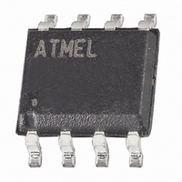
ATTINY15L-1SC Atmel, ATTINY15L-1SC Datasheet - Page 47

ATTINY15L-1SC
Manufacturer Part Number
ATTINY15L-1SC
Description
IC AVR MCU 1K FLASH 2.7V SO8
Manufacturer
Atmel
Series
AVR® ATtinyr
Specifications of ATTINY15L-1SC
Core Processor
AVR
Core Size
8-Bit
Speed
1.6MHz
Peripherals
Brown-out Detect/Reset, POR, PWM, WDT
Number Of I /o
6
Program Memory Size
1KB (512 x 16)
Program Memory Type
FLASH
Eeprom Size
64 x 8
Voltage - Supply (vcc/vdd)
2.7 V ~ 5.5 V
Data Converters
A/D 4x10b
Oscillator Type
Internal
Operating Temperature
0°C ~ 70°C
Package / Case
8-SOIC (5.3mm Width), 8-SOP, 8-SOEIAJ
Lead Free Status / RoHS Status
Contains lead / RoHS non-compliant
Ram Size
-
Connectivity
-
Available stocks
Company
Part Number
Manufacturer
Quantity
Price
Company:
Part Number:
ATTINY15L-1SC
Manufacturer:
ATMEL
Quantity:
3 447
Part Number:
ATTINY15L-1SC
Manufacturer:
ATMEL/爱特梅尔
Quantity:
20 000
The ADC Control and Status
Register – ADCSR
1187H–AVR–09/07
• Bits 4..3 – Res: Reserved Bits
These bits are reserved bits in the ATtiny15L and always read as zero.
• Bits 2..0 – MUX2..MUX0: Analog Channel and Gain Selection Bits 2..0
The value of these bits selects which analog input is connected to the ADC. In case of
differential input (PB3 - PB4), gain selection is also made with these bits. Selecting PB3
as both inputs to the differential gain stage enables offset measurements. Refer to Table
20 for details. If these bits are changed during a conversion, the change will not go into
effect until this conversion is complete (ADIF in ADCSR is set).
Table 20. Input Channel and Gain Selections
Note:
• Bit 7 – ADEN: ADC Enable
Writing a logical “1” to this bit enables the ADC. By clearing this bit to zero, the ADC is
turned off. Turning the ADC off while a conversion is in progress will terminate this
conversion.
• Bit 6 – ADSC: ADC Start Conversion
In Single Conversion mode, a logical “1” must be written to this bit to start each conver-
sion. In Free Running mode, a logical “1” must be written to this bit to start the first
conversion.
When the conversion completes, ADSC returns to zero in Single Conversion mode and
stays high in Free Running mode.
Writing a “0” to this bit has no effect.
• Bit 5 – ADFR: ADC Free Running Select
When this bit is set (one), the ADC operates in Free Running mode. In this mode, the
ADC samples and updates the Data Registers continuously. Clearing this bit (zero) will
terminate Free Running mode. If active channels are used (MUX2 in ADMUX set), the
Bit
$06
Read/Write
Initial Value
MUX2..0
100
101
000
001
010
011
110
111
(1)
(1)
1. For offset calibration only. See “Operation” on page 42.
Single-ended
ADEN
ADC0 (PB5)
ADC1 (PB2)
ADC2 (PB3)
ADC3 (PB4)
R/W
7
0
Input
N/A
ADSC
R/W
6
0
ADFR
R/W
5
0
Differential Input
ADC2 (PB3)
ADC2 (PB3)
ADC2 (PB3)
ADC2 (PB3)
Positive
ADIF
R/W
4
0
ADIE
R/W
3
0
ADPS2
R/W
N/A
2
0
Differential Input
ADC2 (PB3)
ADC2 (PB3)
ADC3 (PB4)
ADC3 (PB4)
ADPS1
Negative
R/W
1
0
ATtiny15L
ADPS0
R/W
0
0
ADCSR
Gain
20x
20x
1x
1x
47


