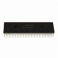
HD6473258P10V Renesas Electronics America, HD6473258P10V Datasheet - Page 201

HD6473258P10V
Manufacturer Part Number
HD6473258P10V
Description
MCU 5V 32K PB-FREE 64-DIP
Manufacturer
Renesas Electronics America
Series
H8® H8/325r
Specifications of HD6473258P10V
Core Size
8-Bit
Program Memory Size
32KB (32K x 8)
Oscillator Type
External
Core Processor
H8/300
Speed
10MHz
Connectivity
SCI, UART/USART
Number Of I /o
53
Program Memory Type
OTP
Ram Size
1K x 8
Voltage - Supply (vcc/vdd)
4.5 V ~ 5.5 V
Operating Temperature
-20°C ~ 75°C
Package / Case
64-DIP
No. Of I/o's
53
Ram Memory Size
1024Byte
Cpu Speed
10MHz
No. Of Timers
3
Digital Ic Case Style
DIP
Supply Voltage
RoHS Compliant
Controller Family/series
H8/330
Rohs Compliant
Yes
Lead Free Status / RoHS Status
Lead free / RoHS Compliant
Eeprom Size
-
Data Converters
-
Peripherals
-
Lead Free Status / RoHS Status
Lead free / RoHS Compliant
Available stocks
Company
Part Number
Manufacturer
Quantity
Price
Company:
Part Number:
HD6473258P10V
Manufacturer:
RENESAS
Quantity:
600
Part Number:
HD6473258P10V
Manufacturer:
HITACHI/日立
Quantity:
20 000
- Current page: 201 of 301
- Download datasheet (2Mb)
(3) Line Break Detection: When the RxD pin receives a continuous stream of 0’s in asynchro-
nous mode (line-break state), a framing error occurs because the SCI detects a 0 stop bit. The value
H’00 is transferred from the RSR to the RDR. Software can detect the line-break state as a framing
error accompanied by H’00 data in the RDR.
The SCI continues to receive data, so if the FER bit is cleared to 0 another framing error will occur.
(4) Sampling Timing and Receive Margin in Asynchronous Mode: The serial clock used by
the SCI in asynchronous mode runs at 16 times the baud rate. The falling edge of the start bit is
detected by sampling the RxD input on the falling edge of this clock. After the start bit is detected,
each bit of receive data in the frame (including the start bit, parity bit, and stop bit or bits) is
sampled on the rising edge of the serial clock pulse at the center of the bit. See figure 9-6.
It follows that the receive margin can be calculated as in equation (1).
When the absolute frequency deviation of the clock signal is 0 and the clock duty factor is 0.5, data
can theoretically be received with distortion up to the margin given by equation (2). This is a
theoretical limit, however. In practice, system designers should allow a margin of 20% to 30%.
194
Related parts for HD6473258P10V
Image
Part Number
Description
Manufacturer
Datasheet
Request
R

Part Number:
Description:
KIT STARTER FOR M16C/29
Manufacturer:
Renesas Electronics America
Datasheet:

Part Number:
Description:
KIT STARTER FOR R8C/2D
Manufacturer:
Renesas Electronics America
Datasheet:

Part Number:
Description:
R0K33062P STARTER KIT
Manufacturer:
Renesas Electronics America
Datasheet:

Part Number:
Description:
KIT STARTER FOR R8C/23 E8A
Manufacturer:
Renesas Electronics America
Datasheet:

Part Number:
Description:
KIT STARTER FOR R8C/25
Manufacturer:
Renesas Electronics America
Datasheet:

Part Number:
Description:
KIT STARTER H8S2456 SHARPE DSPLY
Manufacturer:
Renesas Electronics America
Datasheet:

Part Number:
Description:
KIT STARTER FOR R8C38C
Manufacturer:
Renesas Electronics America
Datasheet:

Part Number:
Description:
KIT STARTER FOR R8C35C
Manufacturer:
Renesas Electronics America
Datasheet:

Part Number:
Description:
KIT STARTER FOR R8CL3AC+LCD APPS
Manufacturer:
Renesas Electronics America
Datasheet:

Part Number:
Description:
KIT STARTER FOR RX610
Manufacturer:
Renesas Electronics America
Datasheet:

Part Number:
Description:
KIT STARTER FOR R32C/118
Manufacturer:
Renesas Electronics America
Datasheet:

Part Number:
Description:
KIT DEV RSK-R8C/26-29
Manufacturer:
Renesas Electronics America
Datasheet:

Part Number:
Description:
KIT STARTER FOR SH7124
Manufacturer:
Renesas Electronics America
Datasheet:

Part Number:
Description:
KIT STARTER FOR H8SX/1622
Manufacturer:
Renesas Electronics America
Datasheet:

Part Number:
Description:
KIT DEV FOR SH7203
Manufacturer:
Renesas Electronics America
Datasheet:


