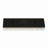
HD6473258P10V Renesas Electronics America, HD6473258P10V Datasheet - Page 127

HD6473258P10V
Manufacturer Part Number
HD6473258P10V
Description
MCU 5V 32K PB-FREE 64-DIP
Manufacturer
Renesas Electronics America
Series
H8® H8/325r
Specifications of HD6473258P10V
Core Size
8-Bit
Program Memory Size
32KB (32K x 8)
Oscillator Type
External
Core Processor
H8/300
Speed
10MHz
Connectivity
SCI, UART/USART
Number Of I /o
53
Program Memory Type
OTP
Ram Size
1K x 8
Voltage - Supply (vcc/vdd)
4.5 V ~ 5.5 V
Operating Temperature
-20°C ~ 75°C
Package / Case
64-DIP
No. Of I/o's
53
Ram Memory Size
1024Byte
Cpu Speed
10MHz
No. Of Timers
3
Digital Ic Case Style
DIP
Supply Voltage
RoHS Compliant
Controller Family/series
H8/330
Rohs Compliant
Yes
Lead Free Status / RoHS Status
Lead free / RoHS Compliant
Eeprom Size
-
Data Converters
-
Peripherals
-
Lead Free Status / RoHS Status
Lead free / RoHS Compliant
Available stocks
Company
Part Number
Manufacturer
Quantity
Price
Company:
Part Number:
HD6473258P10V
Manufacturer:
RENESAS
Quantity:
600
Part Number:
HD6473258P10V
Manufacturer:
HITACHI/日立
Quantity:
20 000
- Current page: 127 of 301
- Download datasheet (2Mb)
Bit 2—Busy Enable (BSE): This bit enables or disables output of the busy signal. Do not set BSE
to 1 in the expanded modes (modes 1 and 2).
Bit 2
ISIE
0
1
Bits 1 and 0—Reserved: These bits cannot be modified and are always read as 1.
6.3 Operation
6.3.1 Output Timing of Output Strobe Signal
The output strobe signal is output when the port 3 data register (P3DR) is written or read. The
output strobe signal goes low at the seventh system clock cycle after P3DR is written or read,
remains low for eight system clock cycles, then goes high. Figure 6-2 shows how the output strobe
signal is output after P3DR is written (when OSS = 1).
Note the following point when reading or writing P3DR twice consecutively.
If P3DR is written or read once, then written or read again within 15 states, the output strobe signal
is not output for the second write or read. Figure 6-3 shows an example of this when OSS = 1.
Port 3
Ø
OS
Description
Busy signal output is disabled.
Busy signal output is enabled.
Port 3 write
Figure 6-2. Output Strobe Output Timing (When OSS = 1)
7 system clocks
8 system clocks
118
(Initial value)
Related parts for HD6473258P10V
Image
Part Number
Description
Manufacturer
Datasheet
Request
R

Part Number:
Description:
KIT STARTER FOR M16C/29
Manufacturer:
Renesas Electronics America
Datasheet:

Part Number:
Description:
KIT STARTER FOR R8C/2D
Manufacturer:
Renesas Electronics America
Datasheet:

Part Number:
Description:
R0K33062P STARTER KIT
Manufacturer:
Renesas Electronics America
Datasheet:

Part Number:
Description:
KIT STARTER FOR R8C/23 E8A
Manufacturer:
Renesas Electronics America
Datasheet:

Part Number:
Description:
KIT STARTER FOR R8C/25
Manufacturer:
Renesas Electronics America
Datasheet:

Part Number:
Description:
KIT STARTER H8S2456 SHARPE DSPLY
Manufacturer:
Renesas Electronics America
Datasheet:

Part Number:
Description:
KIT STARTER FOR R8C38C
Manufacturer:
Renesas Electronics America
Datasheet:

Part Number:
Description:
KIT STARTER FOR R8C35C
Manufacturer:
Renesas Electronics America
Datasheet:

Part Number:
Description:
KIT STARTER FOR R8CL3AC+LCD APPS
Manufacturer:
Renesas Electronics America
Datasheet:

Part Number:
Description:
KIT STARTER FOR RX610
Manufacturer:
Renesas Electronics America
Datasheet:

Part Number:
Description:
KIT STARTER FOR R32C/118
Manufacturer:
Renesas Electronics America
Datasheet:

Part Number:
Description:
KIT DEV RSK-R8C/26-29
Manufacturer:
Renesas Electronics America
Datasheet:

Part Number:
Description:
KIT STARTER FOR SH7124
Manufacturer:
Renesas Electronics America
Datasheet:

Part Number:
Description:
KIT STARTER FOR H8SX/1622
Manufacturer:
Renesas Electronics America
Datasheet:

Part Number:
Description:
KIT DEV FOR SH7203
Manufacturer:
Renesas Electronics America
Datasheet:


