COP8CCE9IMT7/NOPB National Semiconductor, COP8CCE9IMT7/NOPB Datasheet - Page 52
COP8CCE9IMT7/NOPB
Manufacturer Part Number
COP8CCE9IMT7/NOPB
Description
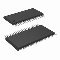
MCU 8BIT FLASH 8K MEM 48-TSSOP
Manufacturer
National Semiconductor
Series
COP8™ 8Cr
Datasheet
1.I2C-CPEV.pdf
(80 pages)
Specifications of COP8CCE9IMT7/NOPB
Core Processor
COP8
Core Size
8-Bit
Speed
10MHz
Connectivity
Microwire/Plus (SPI), UART/USART
Peripherals
Brown-out Detect/Reset, POR, PWM, WDT
Number Of I /o
39
Program Memory Size
8KB (8K x 8)
Program Memory Type
FLASH
Ram Size
256 x 8
Voltage - Supply (vcc/vdd)
2.7 V ~ 5.5 V
Data Converters
A/D 16x10b
Oscillator Type
Internal
Operating Temperature
-40°C ~ 125°C
Package / Case
48-TSSOP
Data Bus Width
8 bit
Maximum Clock Frequency
10 MHz
Data Ram Size
256 B
On-chip Adc
10 bit, 16 channel
Number Of Programmable I/os
37
Number Of Timers
2
Height
0.9 mm
Interface Type
SPI, USART
Length
12.5 mm
Maximum Operating Temperature
+ 125 C
Minimum Operating Temperature
- 40 C
Supply Voltage (max)
5.5 V
Supply Voltage (min)
2.7 V
Width
6.1 mm
Lead Free Status / RoHS Status
Lead free / RoHS Compliant
Eeprom Size
-
Lead Free Status / Rohs Status
Details
Other names
COP8CCE9IMT7


www.national.com
15.0 A/D Converter
Note 20: This Input Channel Selection should not be used when the Multiplexor Output is enabled.
Note 21: This Input Channel Selection should not be used in Differential Mode when the Multiplexor Output is enabled.
15.1.1.2 MULTIPLEXOR OUTPUT SELECT
This 1-bit field allows the output of the A/D multiplexor and
the input to the A/D to be connected directly to external pins.
This allows for an external, common filter/signal conditioning
circuit to be applied to all channels. The output of the exter-
nal conditioning circuit can then be connected directly to the
input of the Sample and Hold input on the A/D Converter.
See Figure 26 for the single ended mode diagram. The
Multiplexor output is connected to ADCH14 and the A/D
input is connected to ADCH15. For Differential mode, the
differential multiplexor outputs are available and should be
converted to a single ended voltage for connection to the A/D
Converter Input. See Figure 27.
The channel assignments for this mode are shown in Table
22.
When using the Mux Output feature, the delay though the
internal multiplexor to the pin, plus the delay of the external
filter circuit, plus the internal delay to the Sample and Hold
will exceed the three clock cycles that’s allowed in the con-
version. This adds the requirement that, whenever the MUX
bit = 1, that the channel selected by ADCH3:0 bits be en-
abled, even when ADBSY = 0, and gated to the mux output
pin. The input path to the A/D converter is also enabled. This
ADCH3
0
0
0
0
0
0
0
0
1
1
1
1
1
1
1
1
ADCH2
TABLE 21. A/D Converter Channel Selection when the Multiplexor Output is Enabled
0
0
0
0
1
1
1
1
0
0
0
0
1
1
1
1
Select Bits
(Continued)
ADCH1
0
0
1
1
0
0
1
1
0
0
1
1
0
0
1
1
ADCH0
0
1
0
1
0
1
0
1
0
1
0
1
0
1
0
1
52
Single Ended Mode
A/D Input (Note 20)
allows the input channel to be selected and settled before
starting a conversion. The sequence to perform conversions
using the Mux Out feature is a multistep process and is listed
below.
1. Select the desired channel and operating modes and
2. Wait the appropriate time until the analog input has
3. Select the same desired channel and operating modes
4. Poll ADBSY until it is cleared by the hardware. This
5. Obtain the results from the result registers.
The port pins used for the multiplexor output must be con-
figured as high impedance inputs. If the port pins are con-
figured as outputs, or as inputs with weak pull-up, there will
be a conflict between the analog signal output and the
digitally driven output.
Mode Select
Channel No.
ADMOD = 0
Mux Output
ADCH14 is
ADCH15 is
(Note 20)
load them into ENAD without setting ADBSY.
settled. This will depend on the application and the
response of the external circuit.
used in step 1 and load them into ENAD and also set
ADBSY or set ADBSY by using the SBIT instruction.
This will start the conversion.
indicates the completion of the conversion.
10
12
13
11
0
1
2
3
4
5
6
7
8
9
Channel Pairs (+, −)
Not Used (Note 21)
A/D Input (Note 20)
Differential Mode
Mux Output −
Mux Output +
Mode Select
ADMOD = 1
ADCH14 is
ADCH15 is
ADC13 is
(Note 21)
(Note 20)
10, 11
11, 10
0, 1
1, 0
2, 3
3, 2
4, 5
5, 4
6, 7
7, 6
8, 9
9, 8
Mux Output
Enabled
MUX
1
1
1
1
1
1
1
1
1
1
1
1
1
1
1
1
Related parts for COP8CCE9IMT7/NOPB
Image
Part Number
Description
Manufacturer
Datasheet
Request
R

Part Number:
Description:
National Semiconductor [8-Bit D/A Converter]
Manufacturer:
National Semiconductor
Datasheet:
Part Number:
Description:
National Semiconductor [Media Coprocessor]
Manufacturer:
National Semiconductor
Datasheet:
Part Number:
Description:
Digitally Controlled Tone and Volume Circuit with Stereo Audio Power Amplifier, Microphone Preamp Stage and National 3D Sound
Manufacturer:
National Semiconductor
Datasheet:
Part Number:
Description:
Digitally Controlled Tone and Volume Circuit with Stereo Audio Power Amplifier, Microphone Preamp Stage and National 3D Sound
Manufacturer:
National Semiconductor
Datasheet:
Part Number:
Description:
AC97 Rev 2 Codec with Sample Rate Conversion and National 3D Sound
Manufacturer:
National Semiconductor
Part Number:
Description:
Manufacturer:
National Semiconductor
Datasheet:
Part Number:
Description:
Manufacturer:
National Semiconductor
Datasheet:
Part Number:
Description:
General Purpose, Low Voltage, Low Power, Rail-to-Rail Output Operational Amplifiers
Manufacturer:
National Semiconductor
Datasheet:
Part Number:
Description:
8-bit 20 MSPS flash A/D converter.
Manufacturer:
National Semiconductor
Datasheet:
Part Number:
Description:
Low Noise Quad Operational Amplifier
Manufacturer:
National Semiconductor
Datasheet:
Part Number:
Description:
Quad Differential Line Receivers
Manufacturer:
National Semiconductor
Datasheet:
Part Number:
Description:
Quad High Speed Trapezoidal? Bus Transceiver
Manufacturer:
National Semiconductor
Datasheet:
Part Number:
Description:
Dual Line Receiver
Manufacturer:
National Semiconductor
Datasheet:
Part Number:
Description:
TTL to 10k ECL Level Translator with Latch
Manufacturer:
National Semiconductor
Datasheet: