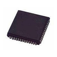
MC68HC711E9MFNE2 Freescale Semiconductor, MC68HC711E9MFNE2 Datasheet - Page 42

MC68HC711E9MFNE2
Manufacturer Part Number
MC68HC711E9MFNE2
Description
IC MCU 8BIT 512BYTES ROM 52-PLCC
Manufacturer
Freescale Semiconductor
Series
HC11r
Specifications of MC68HC711E9MFNE2
Core Processor
HC11
Core Size
8-Bit
Speed
2MHz
Connectivity
SCI, SPI
Peripherals
POR, WDT
Number Of I /o
38
Program Memory Size
12KB (12K x 8)
Program Memory Type
OTP
Eeprom Size
512 x 8
Ram Size
512 x 8
Voltage - Supply (vcc/vdd)
4.5 V ~ 5.5 V
Data Converters
A/D 8x8b
Oscillator Type
Internal
Operating Temperature
-40°C ~ 125°C
Package / Case
52-PLCC
Processor Series
HC711E
Core
HC11
Data Bus Width
8 bit
Data Ram Size
512 B
Interface Type
SCI, SPI
Maximum Clock Frequency
2 MHz
Number Of Programmable I/os
38
Number Of Timers
8
Maximum Operating Temperature
+ 125 C
Mounting Style
SMD/SMT
Minimum Operating Temperature
- 40 C
On-chip Adc
8 bit
Lead Free Status / RoHS Status
Lead free / RoHS Compliant
Available stocks
Company
Part Number
Manufacturer
Quantity
Price
Company:
Part Number:
MC68HC711E9MFNE2
Manufacturer:
TI
Quantity:
167
Company:
Part Number:
MC68HC711E9MFNE2
Manufacturer:
Freescale Semiconductor
Quantity:
10 000
- Current page: 42 of 336
- Download datasheet (4Mb)
Pin Descriptions
2.13.3 Port C
Technical Data
42
While in single-chip operating modes, all port C pins are
general-purpose I/O pins. Port C inputs can be latched into an alternate
PORTCL register by providing an input transition to the STRA signal.
Port C can also be used in full handshake modes of parallel I/O where
the STRA input and STRB output act as handshake control lines.
When in expanded multiplexed modes, all port C pins are configured as
multiplexed address/data signals. During the address portion of each
MCU cycle, bits 7–0 of the address are output on the PC7–PC0 pins.
During the data portion of each MCU cycle (E high), PC7–PC0 are
bidirectional data signals, DATA7–DATA0. The direction of data at the
port C pins is indicated by the R/W signal.
The CWOM control bit in the PIOC register disables the port C P-channel
output driver. CWOM simultaneously affects all eight bits of port C.
Because the N-channel driver is not affected by CWOM, setting CWOM
causes port C to become an open-drain type output port suitable for
wired-OR operation.
It is customary to have an external pullup resistor on lines that are driven
by open-drain devices. Port C can only be configured for wired-OR
operation when the MCU is in single-chip mode. Refer to
Parallel Input/Output (I/O) Ports
functions.
In wired-OR mode:
•
•
When a port C bit is at logic level 0, it is driven low by the
N-channel driver.
When a port C bit is at logic level 1, the associated pin has
high-impedance, as neither the N-channel nor the P-channel
devices are active.
Pin Descriptions
for additional information about port C
M68HC11E Family — Rev. 3.2
Section 6.
MOTOROLA
Related parts for MC68HC711E9MFNE2
Image
Part Number
Description
Manufacturer
Datasheet
Request
R

Part Number:
Description:
APPENDIX A ELECTRICAL CHARACTERISTICS
Manufacturer:
FREESCALE [Freescale Semiconductor, Inc]
Datasheet:
Part Number:
Description:
Manufacturer:
Freescale Semiconductor, Inc
Datasheet:
Part Number:
Description:
Manufacturer:
Freescale Semiconductor, Inc
Datasheet:
Part Number:
Description:
Manufacturer:
Freescale Semiconductor, Inc
Datasheet:
Part Number:
Description:
Manufacturer:
Freescale Semiconductor, Inc
Datasheet:
Part Number:
Description:
Manufacturer:
Freescale Semiconductor, Inc
Datasheet:
Part Number:
Description:
Manufacturer:
Freescale Semiconductor, Inc
Datasheet:
Part Number:
Description:
Manufacturer:
Freescale Semiconductor, Inc
Datasheet:
Part Number:
Description:
Manufacturer:
Freescale Semiconductor, Inc
Datasheet:
Part Number:
Description:
Manufacturer:
Freescale Semiconductor, Inc
Datasheet:
Part Number:
Description:
Manufacturer:
Freescale Semiconductor, Inc
Datasheet:
Part Number:
Description:
Manufacturer:
Freescale Semiconductor, Inc
Datasheet:
Part Number:
Description:
Manufacturer:
Freescale Semiconductor, Inc
Datasheet:
Part Number:
Description:
Manufacturer:
Freescale Semiconductor, Inc
Datasheet:
Part Number:
Description:
Manufacturer:
Freescale Semiconductor, Inc
Datasheet:


