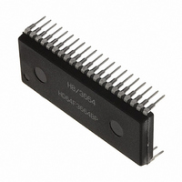
M38513E4FP#U0 Renesas Electronics America, M38513E4FP#U0 Datasheet - Page 28

M38513E4FP#U0
Manufacturer Part Number
M38513E4FP#U0
Description
IC 740 MCU ROM 16K 42SSOP
Manufacturer
Renesas Electronics America
Series
740/38000r
Specifications of M38513E4FP#U0
Core Processor
740
Core Size
8-Bit
Speed
8MHz
Connectivity
SIO, UART/USART
Peripherals
PWM, WDT
Number Of I /o
34
Program Memory Size
16KB (16K x 8)
Program Memory Type
OTP
Ram Size
512 x 8
Voltage - Supply (vcc/vdd)
2.7 V ~ 5.5 V
Data Converters
A/D 5x10b
Oscillator Type
External
Operating Temperature
-20°C ~ 85°C
Package / Case
42-SSOP
Package
42SSOP
Family Name
740
Maximum Speed
8 MHz
Operating Supply Voltage
5 V
Data Bus Width
8 Bit
Number Of Programmable I/os
34
Interface Type
I2C-BUS
On-chip Adc
5-chx10-bit
Number Of Timers
4
Lead Free Status / RoHS Status
Contains lead / RoHS non-compliant
Eeprom Size
-
•Bit 6: Communication mode specification bit (transfer direc-
This bit decides a direction of transfer for data communication.
When this bit is “0,” the reception mode is selected and the data of
a transmitting device is received. When the bit is “1,” the transmis-
sion mode is selected and address data and control data are
output onto the SDA in synchronization with the clock generated
on the S
This bit is set/reset by software and hardware. About set/reset by
hardware is described below. This bit is set to “1” by hardware
when all the following conditions are satisfied:
• When ALS is “0”
• In the slave reception mode or the slave transmission mode
• When the R/W bit reception is “1”
This bit is set to “0” in one of the following conditions:
• When arbitration lost is detected.
• When a STOP condition is detected.
• When writing “1” to this bit by software is invalid by the START
• With MST = “0” and when a START condition is detected.
• With MST = “0” and when ACK non-return is detected.
• At reset
•Bit 7: Communication mode specification bit (master/slave
This bit is used for master/slave specification for data communica-
tion. When this bit is “0,” the slave is specified, so that a START
condition and a STOP condition generated by the master are re-
ceived, and data communication is performed in synchronization
with the clock generated by the master. When this bit is “1,” the
master is specified and a START condition and a STOP condition
are generated. Additionally, the clocks required for data communi-
cation are generated on the SCL.
This bit is set to “0” in one of the following conditions.
• Immediately after completion of 1-byte data transfer when arbi-
• When a STOP condition is detected.
• Writing “1” to this bit by software is invalid by the START condi-
• At reset
Note: START condition duplication preventing function
condition duplication preventing function (Note).
tration lost is detected
tion duplication preventing function (Note).
The MST, TRX, and BB bits is set to “1” at the same time after con-
firming that the BB flag is “0” in the procedure of a START condition
occurrence. However, when a START condition by another master
device occurs and the BB flag is set to “1” immediately after the con-
tents of the BB flag is confirmed, the START condition duplication
preventing function makes the writing to the MST and TRX bits in-
valid. The duplication preventing function becomes valid from the
rising of the BB flag to reception completion of slave address.
tion specification bit: TRX)
specification bit: MST)
CL
.
Fig. 25 Interrupt request signal generating timing
Fig. 24 Structure of I
MST
b7
Note: These bits and flags can be read out, but cannot
IICIRQ
TRX BB PIN AL AAS AD0 LRB
PIN
S
CL
be written.
Write “0” to these bits at writing.
SINGLE-CHIP 8-BIT CMOS MICROCOMPUTER
MITSUBISHI MICROCOMPUTERS
2
C status register
b0
(Built-in 16 KB ROM)
I
(S1 : address 002D
Last receive bit (Note)
General call detecting flag
(Note)
Slave address comparison flag
(Note)
Arbitration lost detecting flag
(Note)
SCL pin low hold bit
Bus busy flag
Communication mode
specification bits
2
C status register
0 : Last bit = “0”
1 : Last bit = “1”
0 : No general call detected
1 : General call detected
0 : Address disagreement
1 : Address agreement
0 : Not detected
1 : Detected
0 : SCL pin low hold
1 : SCL pin low release
0 : Bus free
1 : Bus busy
00 : Slave receive mode
01 : Slave transmit mode
10 : Master receive mode
11 : Master transmit mode
3851 Group
16
)
25


