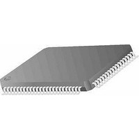
MC68HC11K1CFUE3 Freescale Semiconductor, MC68HC11K1CFUE3 Datasheet - Page 237

MC68HC11K1CFUE3
Manufacturer Part Number
MC68HC11K1CFUE3
Description
MCU 8-BIT 768 RAM 3MHZ 80-QFP
Manufacturer
Freescale Semiconductor
Series
HC11r
Specifications of MC68HC11K1CFUE3
Core Processor
HC11
Core Size
8-Bit
Speed
3MHz
Connectivity
SCI, SPI
Peripherals
POR, PWM, WDT
Number Of I /o
37
Program Memory Type
ROMless
Eeprom Size
640 x 8
Ram Size
768 x 8
Voltage - Supply (vcc/vdd)
4.5 V ~ 5.5 V
Data Converters
A/D 8x8b
Oscillator Type
Internal
Operating Temperature
-40°C ~ 85°C
Package / Case
80-QFP
Data Bus Width
8 bit
Data Ram Size
768 B
Interface Type
SCI, SPI
Maximum Clock Frequency
4 MHz
Number Of Programmable I/os
37
Number Of Timers
8
Maximum Operating Temperature
+ 85 C
Mounting Style
SMD/SMT
Minimum Operating Temperature
- 40 C
On-chip Adc
8 bit, 8 Channel
Lead Free Status / RoHS Status
Lead free / RoHS Compliant
Program Memory Size
-
Lead Free Status / Rohs Status
Details
Available stocks
Company
Part Number
Manufacturer
Quantity
Price
Company:
Part Number:
MC68HC11K1CFUE3
Manufacturer:
FREESCALE
Quantity:
8 831
Company:
Part Number:
MC68HC11K1CFUE3
Manufacturer:
Freescale Semiconductor
Quantity:
10 000
- Current page: 237 of 290
- Download datasheet (4Mb)
11.3.2.4 Memory Mapping Window Control Registers
M68HC11K Family
MOTOROLA
Address: $0058
Address: $0059
Each of the memory mapping window control registers (MM1CR and
MM2CR) determine the active memory bank for the corresponding
window, containing the value to be output on the expansion address
lines when the CPU selects addresses within its extended memory
window. To change banks, write the address of the new bank into the
appropriate window register.
X1A[18:13] — Memory Mapping Window 1 Expansion Address Line
X2A[18:13] — Memory Mapping Window 2 Expansion Address Line
Reset:
Reset:
Read:
Read:
Write:
Write:
Each bit value written to the MMxCR registers is driven on the
corresponding port G expansion address line (if enabled by PGAR) to
enable the specified bank in the window.
Freescale Semiconductor, Inc.
For More Information On This Product,
Memory Expansion and Chip Selects
Bit 7
0
0
0
0
Figure 11-4. Memory Mapping Window Control
Go to: www.freescale.com
Memory Mapping Window 1 Control Register (MM1CR)
Memory Mapping Window 2 Control Register (MM1CR)
Select Bits
Select Bits
X1A18
X2A18
Registers (MM1CR and MM2CR)
6
0
0
X1A17
X2A17
5
0
0
X1A16
X2A16
4
0
0
Memory Expansion and Chip Selects
X1A15
X2A15
3
0
0
X1A14
X2A14
2
0
0
Memory Expansion
X1A13
X2A13
1
0
0
Technical Data
Bit 0
0
0
0
0
237
Related parts for MC68HC11K1CFUE3
Image
Part Number
Description
Manufacturer
Datasheet
Request
R

Part Number:
Description:
MC68HC11 EEPROM Programming from a Personal Computer
Manufacturer:
Motorola / Freescale Semiconductor
Part Number:
Description:
Manufacturer:
Freescale Semiconductor, Inc
Datasheet:
Part Number:
Description:
Manufacturer:
Freescale Semiconductor, Inc
Datasheet:
Part Number:
Description:
Manufacturer:
Freescale Semiconductor, Inc
Datasheet:
Part Number:
Description:
Manufacturer:
Freescale Semiconductor, Inc
Datasheet:
Part Number:
Description:
Manufacturer:
Freescale Semiconductor, Inc
Datasheet:
Part Number:
Description:
Manufacturer:
Freescale Semiconductor, Inc
Datasheet:
Part Number:
Description:
Manufacturer:
Freescale Semiconductor, Inc
Datasheet:
Part Number:
Description:
Manufacturer:
Freescale Semiconductor, Inc
Datasheet:
Part Number:
Description:
Manufacturer:
Freescale Semiconductor, Inc
Datasheet:
Part Number:
Description:
Manufacturer:
Freescale Semiconductor, Inc
Datasheet:
Part Number:
Description:
Manufacturer:
Freescale Semiconductor, Inc
Datasheet:
Part Number:
Description:
Manufacturer:
Freescale Semiconductor, Inc
Datasheet:
Part Number:
Description:
Manufacturer:
Freescale Semiconductor, Inc
Datasheet:
Part Number:
Description:
Manufacturer:
Freescale Semiconductor, Inc
Datasheet:


