HD64F3664BPV Renesas Electronics America, HD64F3664BPV Datasheet - Page 79
HD64F3664BPV
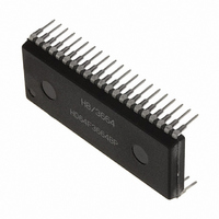
Manufacturer Part Number
HD64F3664BPV
Description
MCU 3/5V 32K,PB-FREE 42-DIP
Manufacturer
Renesas Electronics America
Series
H8® H8/300H Tinyr
Datasheet
1.US3664-BAG1.pdf
(446 pages)
Specifications of HD64F3664BPV
Core Processor
H8/300H
Core Size
16-Bit
Speed
16MHz
Connectivity
I²C, SCI
Peripherals
PWM, WDT
Number Of I /o
29
Program Memory Size
32KB (32K x 8)
Program Memory Type
FLASH
Ram Size
2K x 8
Voltage - Supply (vcc/vdd)
3 V ~ 5.5 V
Data Converters
A/D 8x10b
Oscillator Type
External
Operating Temperature
-20°C ~ 75°C
Package / Case
42-DIP (0.600", 15.24mm)
Lead Free Status / RoHS Status
Lead free / RoHS Compliant
Eeprom Size
-


As a result of this operation, bit 0 in PCR5 becomes 0, making P50 an input port. However, bits 7
and 6 in PCR5 change to 1, so that P57 and P56 change from input pins to output pins. To prevent
this problem, store a copy of the PDR5 data in a work area in memory and manipulate data of the
bit in the work area, then write this data to PDR5.
Prior to executing BCLR
BCLR instruction executed
After executing BCLR
Input/output
Pin state
PCR5
PDR5
RAM0
Input/output
Pin state
PCR5
PDR5
RAM0
MOV.B
MOV.B
MOV.B
BCLR
MOV.B
MOV.B
#0,
#3F,
R0L,
R0L,
@RAM0, R0L
R0L,
P57
Input
Low
level
0
1
0
P57
Input
Low
level
0
1
0
R0L
@RAM0
@PCR5
@RAM0
@PCR5
0
0
0
0
0
0
P56
Input
High
level
P56
Input
High
level
P55
Output
Low
level
1
0
1
P55
Low
level
1
0
1
Output
The PCR5 value (H'3F) is written to a work area in
memory (RAM0) as well as to PCR5.
The BCLR instructions executed for the PCR5 work area
(RAM0).
The work area (RAM0) value is written to PCR5.
P54
Output
Low
level
1
0
1
P54
Output
Low
level
1
0
1
P53
Output
Low
level
1
0
1
P53
Output
Low
level
1
0
1
Rev. 6.00 Mar. 24, 2006 Page 49 of 412
P52
Output
Low
level
1
0
1
P52
Output
Low
level
1
0
1
P51
Output
Low
level
1
0
1
P51
Output
Low
level
1
0
1
REJ09B0142-0600
Section 2 CPU
P50
Output
Low
level
1
0
1
P50
Output
High
level
0
0
0
Related parts for HD64F3664BPV
Image
Part Number
Description
Manufacturer
Datasheet
Request
R


Part Number:
Description:
KIT STARTER FOR M16C/29
Manufacturer:
Renesas Electronics America
Datasheet:

Part Number:
Description:
KIT STARTER FOR R8C/2D
Manufacturer:
Renesas Electronics America
Datasheet:

Part Number:
Description:
R0K33062P STARTER KIT
Manufacturer:
Renesas Electronics America
Datasheet:

Part Number:
Description:
KIT STARTER FOR R8C/23 E8A
Manufacturer:
Renesas Electronics America
Datasheet:

Part Number:
Description:
KIT STARTER FOR R8C/25
Manufacturer:
Renesas Electronics America
Datasheet:

Part Number:
Description:
KIT STARTER H8S2456 SHARPE DSPLY
Manufacturer:
Renesas Electronics America
Datasheet:

Part Number:
Description:
KIT STARTER FOR R8C38C
Manufacturer:
Renesas Electronics America
Datasheet:

Part Number:
Description:
KIT STARTER FOR R8C35C
Manufacturer:
Renesas Electronics America
Datasheet:

Part Number:
Description:
KIT STARTER FOR R8CL3AC+LCD APPS
Manufacturer:
Renesas Electronics America
Datasheet:
Part Number:
Description:
KIT STARTER FOR RX610
Manufacturer:
Renesas Electronics America
Datasheet:

Part Number:
Description:
KIT STARTER FOR R32C/118
Manufacturer:
Renesas Electronics America
Datasheet:

Part Number:
Description:
KIT DEV RSK-R8C/26-29
Manufacturer:
Renesas Electronics America
Datasheet:

Part Number:
Description:
KIT STARTER FOR SH7124
Manufacturer:
Renesas Electronics America
Datasheet:

Part Number:
Description:
KIT STARTER FOR H8SX/1622
Manufacturer:
Renesas Electronics America
Datasheet: