DF2212CUNP24V Renesas Electronics America, DF2212CUNP24V Datasheet - Page 440
DF2212CUNP24V
Manufacturer Part Number
DF2212CUNP24V
Description
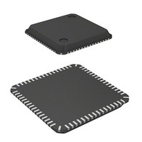
MCU 16BIT FLASH 3V 128K 64-QFN
Manufacturer
Renesas Electronics America
Series
H8® H8S/2200r
Datasheet
1.DF2218UTF24V.pdf
(758 pages)
Specifications of DF2212CUNP24V
Core Processor
H8S/2000
Core Size
16-Bit
Speed
24MHz
Connectivity
SCI, SmartCard, USB
Peripherals
DMA, POR, PWM, WDT
Number Of I /o
37
Program Memory Size
128KB (128K x 8)
Program Memory Type
FLASH
Ram Size
12K x 8
Voltage - Supply (vcc/vdd)
2.7 V ~ 3.6 V
Data Converters
A/D 6x10b
Oscillator Type
External
Operating Temperature
-20°C ~ 75°C
Package / Case
64-QFN
Lead Free Status / RoHS Status
Lead free / RoHS Compliant
Eeprom Size
-
Available stocks
Company
Part Number
Manufacturer
Quantity
Price
Company:

Part Number:
DF2212CUNP24V
Manufacturer:
Renesas Electronics America
Quantity:
135


12.3.9
SEMRA_0 extends the functions of SCI_0. SEMR0 enables selection of the SCI_0 select function
in synchronous mode, base clock setting in asynchronous mode, and also clock source selection
and automatic transfer rate setting. Figure 12.3 shows an example of the internal base clock when
an average transfer rate is selected and figure 12.4 shows as example of the setting when the TPU
clock input is selected.
Rev.7.00 Dec. 24, 2008 Page 384 of 698
REJ09B0074-0700
Bit
7
6
5
4
Bit Name Initial Value R/W Description
SSE
TCS2
TCS1
TCS0
Serial Extended Mode Register A_0 (SEMRA_0)
0
0
0
0
R/W SCI_0 Select Enable
R/W
R/W
R/W
Allows selection of the SCI0 select function when an
external clock is input in synchronous mode.
The SSE setting is valid when external clock input is used
(CKE1 = 1 in SCR) in synchronous mode (C/A = 1 in SMR).
0: SCI_0 select function disabled
1: SCI_0 select function enabled
When the SCI_0 select function is enabled, if 1 is input to
the PG1/IRQ7 pin, TxD0 output goes to the high-impedance
state, SCK0 input is fixed high.
TPU Clock Select
When the TPU clock is input (ACS3 to ACS0 = B'0100) as
the clock source in asynchronous mode, serial transfer
clock is generated depending on the combination of the
TPU clock.
000
001
010
011
1××
&: AND (logical multiplication)
I : OR (logical addition)
Note: The functions of bits 6 to 4 are not supported by the
Legend:
Base Clock
TIOCA1
TIOCA0 | TIOCC0
TIOCA0
TIOCA0 | TIOCC0
Reserved (Setting prohibited)
E6000 emulator. Figure 12.4 shows the setting
examples.
Clock Enable
TIOCA2
TIOCA1
TIOCA1 & TIOCA2
TIOCA1 & TIOCA2
TCLKA
Base clock written
in the left column
Pin input
Pin input
Pin input
TCLKB
Pin input
Base clock written
in the left column
in the left column
Base clock written
in the left column
Base clock written
TCLKC
Pin input
Pin input
Pin input
Pin input
Related parts for DF2212CUNP24V
Image
Part Number
Description
Manufacturer
Datasheet
Request
R

Part Number:
Description:
KIT STARTER FOR M16C/29
Manufacturer:
Renesas Electronics America
Datasheet:

Part Number:
Description:
KIT STARTER FOR R8C/2D
Manufacturer:
Renesas Electronics America
Datasheet:

Part Number:
Description:
R0K33062P STARTER KIT
Manufacturer:
Renesas Electronics America
Datasheet:

Part Number:
Description:
KIT STARTER FOR R8C/23 E8A
Manufacturer:
Renesas Electronics America
Datasheet:

Part Number:
Description:
KIT STARTER FOR R8C/25
Manufacturer:
Renesas Electronics America
Datasheet:

Part Number:
Description:
KIT STARTER H8S2456 SHARPE DSPLY
Manufacturer:
Renesas Electronics America
Datasheet:

Part Number:
Description:
KIT STARTER FOR R8C38C
Manufacturer:
Renesas Electronics America
Datasheet:

Part Number:
Description:
KIT STARTER FOR R8C35C
Manufacturer:
Renesas Electronics America
Datasheet:

Part Number:
Description:
KIT STARTER FOR R8CL3AC+LCD APPS
Manufacturer:
Renesas Electronics America
Datasheet:
Part Number:
Description:
KIT STARTER FOR RX610
Manufacturer:
Renesas Electronics America
Datasheet:

Part Number:
Description:
KIT STARTER FOR R32C/118
Manufacturer:
Renesas Electronics America
Datasheet:

Part Number:
Description:
KIT DEV RSK-R8C/26-29
Manufacturer:
Renesas Electronics America
Datasheet:

Part Number:
Description:
KIT STARTER FOR SH7124
Manufacturer:
Renesas Electronics America
Datasheet:

Part Number:
Description:
KIT STARTER FOR H8SX/1622
Manufacturer:
Renesas Electronics America
Datasheet:

Part Number:
Description:
KIT DEV FOR SH7203
Manufacturer:
Renesas Electronics America
Datasheet: