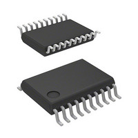
R5F21294SNSP#U0 Renesas Electronics America, R5F21294SNSP#U0 Datasheet - Page 47

R5F21294SNSP#U0
Manufacturer Part Number
R5F21294SNSP#U0
Description
MCU 3/5V 16K+2K 20PIN-SSOP
Manufacturer
Renesas Electronics America
Series
M16C™ M16C/R8C/Tiny/29r
Datasheet
1.R5F21282SNSPU0.pdf
(473 pages)
Specifications of R5F21294SNSP#U0
Core Processor
R8C
Core Size
16-Bit
Speed
20MHz
Connectivity
I²C, LIN, SIO, SSU, UART/USART
Peripherals
LED, POR, Voltage Detect, WDT
Number Of I /o
13
Program Memory Size
16KB (16K x 8)
Program Memory Type
FLASH
Ram Size
1K x 8
Voltage - Supply (vcc/vdd)
2.2 V ~ 5.5 V
Data Converters
A/D 4x10b
Oscillator Type
Internal
Operating Temperature
-20°C ~ 85°C
Package / Case
20-SSOP
Lead Free Status / RoHS Status
Lead free / RoHS Compliant
Eeprom Size
-
Available stocks
Company
Part Number
Manufacturer
Quantity
Price
- Current page: 47 of 473
- Download datasheet (5Mb)
R8C/28 Group, R8C/29 Group
Rev.2.10
REJ09B0279-0210
5.2
Figure 5.8
reset signal
Power V
When the RESET pin is connected to the VCC pin via a pull-up resistor, and the VCC pin voltage level rises while
the rise gradient is trth or more, the power-on reset function is enabled and the MCU resets its pins, CPU, and SFR.
When a capacitor is connected to the RESET pin, too, always keep the voltage to the RESET pin 0.8VCC or more.
When the input voltage to the VCC pin reaches the Vdet0 (Vdet1 for J, K version) level or above, the low-speed
on-chip oscillator clock starts counting. When the low-speed on-chip oscillator clock count reaches 32, the internal
reset signal is held “H” and the MCU enters the reset sequence (refer to Figure 5.4). The low-speed on-chip
oscillator clock divided by 8 is automatically selected as the CPU clock after reset.
Refer to 4. Special Function Registers (SFRs) for the states of the SFR after power-on reset.
The voltage monitor 0 reset is enabled after power-on reset.
Figures 5.8 and 5.9 show the Example of Power-On Reset Circuit and Operation.
NOTES:
(“L” valid)
External
4.7 kΩ
(reference)
Internal
1. When using the voltage monitor 0 digital filter, ensure that the voltage is within the MCU operation voltage
2. The sampling clock can be selected. Refer to 6. Voltage Detection Circuit for details.
3. Vdet0 indicates the voltage detection level of the voltage detection 0 circuit. Refer to 6. Voltage Detection
4. Refer to 20. Electrical Characteristics.
5. To use the power-on reset function, enable voltage monitor 0 reset by setting the LVD0ON bit in the OFS
V
V
det0
Power-On Reset Function
por1
range (2.2 V or above) during the sampling time.
Circuit for details.
register to 0, the VW0C0 and VW0C6 bits in the VW0C register to 1 respectively, and the VCA25 bit in the
VCA2 register to 1.
Sep 26, 2008
CC
(3)
Example of Power-On Reset Circuit and Operation (N, D version)
t
w(por1)
VCC
RESET
Page 28 of 441
t
rth
f
OCO-S
1
Sampling time
× 32
(1, 2)
2.2 V
t
rth
f
OCO-S
V
1
por2
× 32
V
det0
(3)
5. Resets
Related parts for R5F21294SNSP#U0
Image
Part Number
Description
Manufacturer
Datasheet
Request
R

Part Number:
Description:
KIT STARTER FOR M16C/29
Manufacturer:
Renesas Electronics America
Datasheet:

Part Number:
Description:
KIT STARTER FOR R8C/2D
Manufacturer:
Renesas Electronics America
Datasheet:

Part Number:
Description:
R0K33062P STARTER KIT
Manufacturer:
Renesas Electronics America
Datasheet:

Part Number:
Description:
KIT STARTER FOR R8C/23 E8A
Manufacturer:
Renesas Electronics America
Datasheet:

Part Number:
Description:
KIT STARTER FOR R8C/25
Manufacturer:
Renesas Electronics America
Datasheet:

Part Number:
Description:
KIT STARTER H8S2456 SHARPE DSPLY
Manufacturer:
Renesas Electronics America
Datasheet:

Part Number:
Description:
KIT STARTER FOR R8C38C
Manufacturer:
Renesas Electronics America
Datasheet:

Part Number:
Description:
KIT STARTER FOR R8C35C
Manufacturer:
Renesas Electronics America
Datasheet:

Part Number:
Description:
KIT STARTER FOR R8CL3AC+LCD APPS
Manufacturer:
Renesas Electronics America
Datasheet:

Part Number:
Description:
KIT STARTER FOR RX610
Manufacturer:
Renesas Electronics America
Datasheet:

Part Number:
Description:
KIT STARTER FOR R32C/118
Manufacturer:
Renesas Electronics America
Datasheet:

Part Number:
Description:
KIT DEV RSK-R8C/26-29
Manufacturer:
Renesas Electronics America
Datasheet:

Part Number:
Description:
KIT STARTER FOR SH7124
Manufacturer:
Renesas Electronics America
Datasheet:

Part Number:
Description:
KIT STARTER FOR H8SX/1622
Manufacturer:
Renesas Electronics America
Datasheet:

Part Number:
Description:
KIT DEV FOR SH7203
Manufacturer:
Renesas Electronics America
Datasheet:


