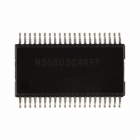
M38503G4AFP#U1 Renesas Electronics America, M38503G4AFP#U1 Datasheet - Page 31

M38503G4AFP#U1
Manufacturer Part Number
M38503G4AFP#U1
Description
IC 740/3850 MCU QZ-ROM 42SSOP
Manufacturer
Renesas Electronics America
Series
740/38000r
Datasheet
1.M38507F8AFPU1.pdf
(61 pages)
Specifications of M38503G4AFP#U1
Core Processor
740
Core Size
8-Bit
Speed
12.5MHz
Connectivity
SIO, UART/USART
Peripherals
PWM, WDT
Number Of I /o
32
Program Memory Size
16KB (16K x 8)
Program Memory Type
QzROM
Ram Size
512 x 8
Voltage - Supply (vcc/vdd)
1.8 V ~ 5.5 V
Data Converters
A/D 9x10b
Oscillator Type
Internal
Operating Temperature
-20°C ~ 85°C
Package / Case
42-SSOP
Lead Free Status / RoHS Status
Lead free / RoHS Compliant
Eeprom Size
-
Available stocks
Company
Part Number
Manufacturer
Quantity
Price
3850 Group (Spec.A QzROM version)
Rev.2.13
REJ03B0125-0213
Fig 26. Block diagram of Serial I/O2
Fig 27. Timing chart of Serial I/O2
P4
P0
P0
P0
Receive enable signal S
Note: Either high-speed, middle-speed or low-speed mode is selected by bits 6 and 7 of CPU mode register.
P0
3
3
1
2
/S
/S
/S
/S
Notes1: When the internal clock is selected as a transfer clock, the f(X
0
Transfer clock (Note 1)
Serial I/O2 output S
/S
X
CMP2
RDY2
OUT2
CLK2
X
CIN
IN2
Serial I/O2 input S
IN
2: When the internal clock is selected as a transfer clock, the S
Main clock division ratio
selection bits (Note)
serial I/O2 register
/INT
Write-in signal to
setting bits 0 to 2 of serial I/O2 control register 1.
Apr 17, 2009
2
Serial I/O2 port selection bit
Serial I/O2
synchronous clock
selection bit
Serial I/O2 I/O comparison
signal control bit
Serial I/O2 port selection bit
S
RDY2
OUT2
RDY2
IN2
output enable bit
“0”
P0
“1”
P0
“0”
“1”
1
3
latch
Page 29 of 56
latch
“1”
“0”
“0”
“00”
“01”
“10”
P4
“1”
P0
S
RDY2
3
2
latch
latch
Synchronous
Q
D
0
circuit
Serial I/O2 synchronous
clock selection bit
External clock
D
D
1
D
“1”
2
OUT2
“0”
IN
Optional transfer bits (3)
Serial I/O counter 2 (3)
) clock division (f(X
pin has high impedance after transfer completion.
Serial I/O2 register (8)
1/8
1/16
1/32
1/64
1/128
1/256
D
3
D
4
CIN
) in low-speed mode) can be selected by
Internal synchronous
clock selection bits
D
5
Serial I/O2 interrupt request bit set
Data bus
D
6
Serial I/O2
interrupt request
D
7
(Note 2)


