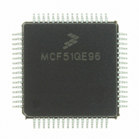
MCF51QE96CLH Freescale Semiconductor, MCF51QE96CLH Datasheet
MCF51QE96CLH
Specifications of MCF51QE96CLH
Available stocks


Related parts for MCF51QE96CLH


MCF51QE96CLH Summary of contents
Page 1
... Illegal opcode and illegal address detection with programmable reset or exception response – Flash block protection Freescale reserves the right to change the detail specifications as may be required to permit improvements in the design of its products. © Freescale Semiconductor, Inc., 2008. All rights reserved. Document Number: MCF51QE128 MCF51QE128 80-LQFP MCF51QE64, ...
Page 2
... AC Characteristics . . . . . . . . . . . . . . . . . . . . . . . . . . . . 21 3.10.1 Control Timing . . . . . . . . . . . . . . . . . . . . . . . . . 21 3.10.2 TPM Module Timing . . . . . . . . . . . . . . . . . . . . . 23 3.10.3 SPI Timing . . . . . . . . . . . . . . . . . . . . . . . . . . . . 24 3.11 Analog Comparator (ACMP) Electricals . . . . . . . . . . . 27 3.12 ADC Characteristics . . . . . . . . . . . . . . . . . . . . . . . . . . 27 3.13 Flash Specifications Ordering Information . . . . . . . . . . . . . . . . . . . . . . . . . . . . . . . 31 5 Package Information . . . . . . . . . . . . . . . . . . . . . . . . . . . . . . . 31 5.1 Mechanical Drawings Product Documentation Revision History . . . . . . . . . . . . . . . . . . . . . . . . . . . . . . . . . . 36 MCF51QE128 Series Data Sheet, Rev. 7 Freescale Semiconductor ...
Page 3
... PTJ1 PTJ0 V REFH V REFL V DDA V SSA PTH7/SDA2 PTH6/SCL2 PTH5 PTH4 PTH3 PTH2 PTH1 PTH0 Freescale Semiconductor TPM1CH2-0 3-CHANNEL TIMER/PWM TPM1CLK MODULE (TPM1) ACMP1O ANALOG COMPARATOR ACMP1+ (ACMP1) ACMP1- EXTAL INTERNAL CLOCK XTAL SOURCE (ICS) OSCILLATOR (XOSC) TPM2CH2-0 3-CHANNEL TIMER/PWM MODULE (TPM2) ...
Page 4
... Ports C and E are shadowed with ColdFire Rapid GPIO module. 4 MCF51QE128 MCF51QE96 131072 98304 8192 8192 yes yes yes yes yes yes yes yes yes yes yes yes yes yes yes MCF51QE128 Series Data Sheet, Rev. 7 MCF51QE64 MCF51QE32 65536 32768 8192 8192 Freescale Semiconductor ...
Page 5
... SS PTB7/SCL1/EXTAL 14 PTB6/SDA1/XTAL 15 PTH3 16 PTH2 17 PTH1 18 PTH0 19 PTE6/RGPIO6 20 Freescale Semiconductor Table 1 Pins in bold are added from the next smaller package. Figure 2. Pin Assignments in 80-Pin LQFP MCF51QE128 Series Data Sheet, Rev. 7 Pin Assignments for pin availability by package pin-count. 60 PTA2/KBI1P2/SDA1/ADP2 59 PTA3/KBI1P3/SCL1/ADP3 58 PTD2/KBI2P2/MISO2 57 PTD3/KBI2P3/SS2 56 ...
Page 6
... PTD0/KBI2P0/SPSCK2 PTH7/SDA2 PTH6/SCL2 PTE7/RGPIO7/TPM3CLK V V DDAD V REFH V REFL V SSAD V PTB7/SCL1/EXTAL PTB6/SDA1/XTAL PTH1 PTH0 PTE6/RGPIO6 Figure 3. Pin Assignments in 64-Pin LQFP Package MCF51QE128 Series Data Sheet, Rev PTA2/KBI1P2/SDA11/ADP2 47 PTA3/KBI1P3/SCL1/ADP3 46 PTD2/KBI2P2/MISO2 45 PTD3/KBI2P3/SS2 44 PTD4/KBI2P4 43 PTF0/ADP10 PTF1/ADP11 PTE4/RGPIO4 39 PTA6/TPM1CH2/ADP8 38 PTA7/TPM2CH2/ADP9 37 PTF2/ADP12 36 PTF3/ADP13 35 PTB0/KBI1P4/RxD1/ADP4 34 PTB1/KBI1P5/TxD1/ADP5 33 Freescale Semiconductor ...
Page 7
... Freescale Semiconductor ←⎯ Lowest Priority Port Pin Alt 1 Alt 2 PTD1 KBI2P1 MOSI2 PTD0 KBI2P0 SPSCK2 PTH7 SDA2 PTH6 SCL2 PTH5 PTH4 PTE7 RGPIO7 TPM3CLK PTB7 SCL1 PTB6 SDA1 PTH3 PTH2 PTH1 PTH0 PTE6 RGPIO6 PTE5 RGPIO5 ...
Page 8
... PTA4 ACMP1O BKGD MCF51QE128 Series Data Sheet, Rev. 7 ⎯→ Highest Alt 3 Alt 4 ADP5 ADP4 ADP13 ADP12 ADP9 ADP8 ADP11 ADP10 ADP3 ADP2 ADP1 ACMP1- ADP0 ACMP1+ ACMP2- ACMP2+ ADP23 ADP22 ADP21 ADP20 ADP19 ADP18 SPSCK1 ACMP2O RSTO RESET MS Freescale Semiconductor ...
Page 9
... Reliability of operation is enhanced if unused inputs are tied to an appropriate logic voltage level (for instance, either the programmable pull-up resistor associated with the pin is enabled Freescale Semiconductor Table 3. Parameter Classifications NOTE MCF51QE128 Series Data Sheet, Rev. 7 Electrical Characteristics 9 ...
Page 10
... MCF51QE128 Series Data Sheet, Rev. 7 Value Unit –0.3 to +3.8 V 120 mA –0 0 ± °C –55 to 150 ) and negative (V ) clamp DD SS and range during instantaneous and > greater than In DD into account in power calculations, determine I will be very small Value Unit – ° ° °C °C/W 47 Freescale Semiconductor ...
Page 11
... Model Series resistance Human Storage capacitance Body Number of pulses per pin Series resistance Machine Storage capacitance Number of pulses per pin Minimum input voltage limit Latch-up Maximum input voltage limit Freescale Semiconductor ) in °C can be obtained from: J × θ ÷ 273° ...
Page 12
... V — — DD — — 0. — — — — — — — SS 17.5 — 52.5 Freescale Semiconductor Unit V — — V — — — — — mV μA 1 μA 1 kΩ ...
Page 13
... Maximum is highest voltage that POR is guaranteed. Low voltage detection and warning limits measured at 1 MHz bus frequency Run at 1 MHz bus frequency 9 Factory trimmed 3.0 V, Temp = 25°C DD Freescale Semiconductor Table 8. DC Characteristics (continued) Symbol Condition Single pin limit I V < ...
Page 14
... MCF51QE128 Series Data Sheet, Rev. 7 PULL-DOWN RESISTOR TYPICALS 85°C 25°C –40°C 2.3 2.8 3.3 3.6 V (V) DD TYPICAL 85° 25°C, OL –40° (V) DD Low Drive (PTxDSn = 0) — TYPICAL 85°C 25°C –40° (V) DD High Drive (PTxDSn = 1) — Freescale Semiconductor 4 ...
Page 15
... Supply Current Characteristics This section includes information about power supply current in various operating modes. Num C Parameter P Run supply current FEI mode, all modules Run supply current FEI mode, all modules off Freescale Semiconductor 3 0.25 0.2 0.15 0.1 0.05 0 –15 – 3.0 V ...
Page 16
... Temperature (°C) - 100 150 1000 1000 1100 1500 100 150 90 100 110 115 106 114 120 Freescale Semiconductor Temp (° Units ...
Page 17
... Not available in stop2 mode 1.8 2 Figure 9. Typical Run I Freescale Semiconductor 2.2 2.4 2.6 VDD (V) for FBE and FEI (ADC off, All Other Modules Enabled) MCF51QE128 Series Data Sheet, Rev. 7 Electrical Characteristics FEI: 24 MHz FBELP: 24 MHz FEI: 8 MHz FBELP: 8 MHz FEI: 1 MHz FBELP: 1 MHz 2 ...
Page 18
... R S — — — — 200 — CSTL — 400 — t — 5 — CSTH — 15 — f 0.03125 — 40.0 extal 0 — 50.33 Freescale Semiconductor Unit kHz MHz MHz MΩ kΩ ms MHz MHz ...
Page 19
... P DMX32 = 1 Resolution of trimmed DCO output frequency at fixed voltage and 6 C temperature (using FTRIM) Resolution of trimmed DCO output frequency at fixed voltage and 7 C temperature (not using FTRIM) Freescale Semiconductor XOSC EXTAL R F Crystal or Resonator C 1 XOSC EXTAL Crystal or Resonator Low range (DRS=00) ...
Page 20
... MCF51QE128 Series Data Sheet, Rev Symbol Min Typ Max + 0.5 Δf ± 2 — dco_t -1.0 Δf ± 0.5 ± 1 — dco_t t — — 1 Acquire C — 0.02 0.2 Jitter Bus percentage for a Jitter 60 80 100 = 3 Freescale Semiconductor Unit %f dco %f dco ms %f dco . 120 ...
Page 21
... Reset low drive BKGD/MS setup time after issuing background debug 5 D force reset to enter user or BDM modes BKGD/MS hold time after issuing background debug 6 D force reset to enter user or BDM modes Freescale Semiconductor 2.7V VDD Table 13. Control Timing Rating Symbol ) Bus f ...
Page 22
... MCF51QE128 Series Data Sheet, Rev Min Typ Max t 100 — — IHIL — — cyc t 100 — — IHIL — — cyc , t Fall — 8 — — 31 — Fall — 7 — — 24 — — 4 — MSH Freescale Semiconductor Unit μs after V DD ...
Page 23
... D External clock frequency 2 D External clock period 3 D External clock high time 4 D External clock low time 5 D Input capture pulse width TCLK TPMCHn TPMCHn Freescale Semiconductor Table 14. TPM Input Timing Function Symbol f TCLK t TCLK t clkh t clkl t ICPW t TCLK t clkh Figure 16 ...
Page 24
... SPSCK 1 — t cyc 1/2 — t SPSCK 1 — t cyc t – 30 1024 t ns cyc cyc t – 30 — ns cyc 15 — — — — ns — cyc — cyc — — — — ns — t – cyc — — t – cyc — Freescale Semiconductor ...
Page 25
... SPSCK (CPOL = 1) (OUTPUT) 5 MISO MSB IN (INPUT) 9 MOSI PORT DATA MASTER MSB OUT (OUTPUT) NOTES output mode (DDS7 = 1, SSOE = 1). 2. LSBF = 0. For LSBF = 1, bit order is LSB, bit 1, ..., bit 6, MSB. Freescale Semiconductor 1 4 BIT LSB BIT Figure 18. SPI Master Timing (CPHA = (2) BIT (2) BIT 6 ...
Page 26
... Not defined but normally LSB of character just received BIT BIT Figure 20. SPI Slave Timing (CPHA = BIT MSB OUT 6 BIT Figure 21. SPI Slave Timing (CPHA = 1) MCF51QE128 Series Data Sheet, Rev SEE SLAVE LSB OUT NOTE LSB SLAVE LSB OUT LSB IN Freescale Semiconductor ...
Page 27
... ADCK f ADCK 8 bit mode (all valid f ADC Conversion High Speed (ADLPC=0) D Clock Freq. Low Power (ADLPC=1) 1 Typical values assume V = 3.0V, Temp = 25°C, f DDAD only and are not tested in production potential difference. Freescale Semiconductor Symbol DDAC V AIN V AIO ALKG t AINIT Table 17. 12-bit ADC Operating Conditions ...
Page 28
... ADIN SIMPLIFIED CHANNEL SELECT CIRCUIT ADC SAR ENGINE R ADIN R ADIN R ADIN R ADIN C ADIN = DDAD REFL SSAD 1 Typ Max Unit Comment 120 — μA 202 — μA 288 — μA 0.532 1 mA μA 0.007 0.8 3 ADACK MHz 2 3.3 Freescale Semiconductor = 1/f ADACK ...
Page 29
... Typical values assume V = 3.0V, Temp = 25°C, f DDAD only and are not tested in production LSB = ( )/2 REFH REFL 3 Monotonicity and No-Missing-Codes guaranteed in 10 bit and 8 bit modes 4 Based on input pad leakage current. Refer to pad electricals. Freescale Semiconductor = REFH DDAD C Symb Min Typ P t — 20 ADC C — ...
Page 30
... MCF51QE128 Series Data Sheet, Rev. 7 supply. For more detailed DD Typical Max 1.8 3.6 1.8 3.6 200 5 6. 4000 20,000 — 9.7 — — 7.6 — — — — 100,000 — 15 100 — Freescale Semiconductor Unit V V kHz μs t Fcyc t Fcyc t Fcyc t Fcyc mA mA cycles years ...
Page 31
... Ordering Information This section contains ordering information for MCF51QE128MCF51QE96, and MCF51QE64 devices. 1 Freescale Part Number MCF51QE128CLK MCF51QE128CLH MCF51QE96CLK MCF51QE96CLH MCF51QE64CLH MCF51QE32CLH MCF51QE32LH 1 See the reference manual, MCF51QE128RM, for a complete description of modules included on each device. 2 See Table 21 for package information. 5 Package Information The below table details the various packages available ...
Page 32
... REF R1 0.10 0.20 0.004 0.008 S 16.00 BSC 0.630 BSC S1 8.00 BSC 0.315 BSC U 0.09 0.16 0.004 0.006 V 16.00 BSC 0.630 BSC V1 8.00 BSC 0.315 BSC W 0.20 REF 0.008 REF Z 1.00 REF 0.039 REF ––– 0 ––– Freescale Semiconductor ...
Page 33
... Figure 24. 64-pin LQFP Package Drawing (Case 840F, Doc #98ASS23234W), Sheet Freescale Semiconductor MCF51QE128 Series Data Sheet, Rev. 7 Package Information 33 ...
Page 34
... Package Information Figure 25. 64-pin LQFP Package Drawing (Case 840F, Doc #98ASS23234W), Sheet MCF51QE128 Series Data Sheet, Rev. 7 Freescale Semiconductor ...
Page 35
... Figure 26. 64-pin LQFP Package Drawing (Case 840F, Doc #98ASS23234W), Sheet Freescale Semiconductor MCF51QE128 Series Data Sheet, Rev. 7 Package Information 35 ...
Page 36
... Table 22. Revision History Description of Changes 8: Changed Condition entires in specs #6 (V ≤ 1. > 2.7V and V > 1.8V Changed V rising and V falling min/typ/max specs in row #19 (Low-voltage DD DD specification’s test category from AIO Thermal Characteristics MCF51QE128 Series Data Sheet, Rev. 7 ≥ 1. and # from Freescale Semiconductor ...
Page 37
... Freescale Semiconductor MCF51QE128 Series Data Sheet, Rev. 7 Revision History 37 ...
Page 38
... Freescale Semiconductor product could create a situation where personal injury or death may occur. Should Buyer ...