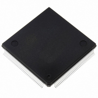
ST10F276Z5Q3TR STMicroelectronics, ST10F276Z5Q3TR Datasheet - Page 33

ST10F276Z5Q3TR
Manufacturer Part Number
ST10F276Z5Q3TR
Description
MCU 16BIT 832KBIT FLASH 144-PQFP
Manufacturer
STMicroelectronics
Series
ST10r
Datasheet
1.ST10F276Z5T3.pdf
(239 pages)
Specifications of ST10F276Z5Q3TR
Core Processor
ST10
Core Size
16-Bit
Speed
64MHz
Connectivity
ASC, CAN, EBI/EMI, I²C, SSC, UART/USART
Peripherals
POR, PWM, WDT
Number Of I /o
111
Program Memory Size
832KB (832K x 8)
Program Memory Type
FLASH
Ram Size
68K x 8
Voltage - Supply (vcc/vdd)
4.5 V ~ 5.5 V
Data Converters
A/D 24x10b
Oscillator Type
Internal
Operating Temperature
-40°C ~ 125°C
Package / Case
144-QFP
Processor Series
ST10F27x
Core
ST10
Data Bus Width
16 bit
Data Ram Size
68 KB
Interface Type
CAN, I2C
Maximum Clock Frequency
64 MHz
Number Of Programmable I/os
111
Number Of Timers
5
Maximum Operating Temperature
+ 125 C
Mounting Style
SMD/SMT
Minimum Operating Temperature
- 40 C
On-chip Adc
10 bit, 24 Channel
For Use With
497-6399 - KIT DEV STARTER ST10F276Z5
Lead Free Status / RoHS Status
Lead free / RoHS Compliant
Eeprom Size
-
Lead Free Status / Rohs Status
Details
Available stocks
Company
Part Number
Manufacturer
Quantity
Price
Company:
Part Number:
ST10F276Z5Q3TR
Manufacturer:
STMicroelectronics
Quantity:
10 000
- Current page: 33 of 239
- Download datasheet (3Mb)
ST10F276Z5
4.4.4
Flash control register 1 high
The Flash control register 1 high (FCR1H), together with Flash control register 1 low
(FCR1L), is used to select the sectors to erase, or during any write operation to monitor the
status of each sector and each bank of the module selected by SMOD bit of FCR0H. First
diagram shows FCR1H meaning when SMOD=0; the second one when SMOD=1.
FCR1H (0x0E 0006) SMOD=0
FCR1H (0x0E 0006) SMOD=1
Table 10.
During any erase operation, these bits are automatically set and give the status of the 2
sectors of Bank 1 (B1F1-B1F0). The meaning of B1Fy bit for sector y of bank 1 is given by
the next
errors are detected.
SMOD=0 (XFLASH selected)
SMOD=1 (IFLASH selected)
15
15
B3F(1:0)
B1F(1:0)
B(3:2)S
B(1:0)S
Bit
14
14
Table
Flash control register 1 high
13
13
reserved
reserved
Bank 3 XFLASH sector 1:0 status
During any erase operation, these bits are automatically set and give the status of the
2 sectors of bank 3 (B3F1-B3F0). The meaning of B3Fy bit for sector y of bank 1 is
given by the next
operation if no errors are detected.
Bank 3-2 status (XFLASH)
During any erase operation, these bits are automatically modified and give the status
of the 2 Banks (B3-B2). The meaning of BxS bit for bank x is given in the next
Table
are detected.
Bank 1 IFLASH sector 1:0 status
During any erase operation, these bits are automatically set and give the status of the
2 sectors of bank 1 (B1F1-B1F0). The meaning of B1Fy bit for sector y of bank 1 is
given by the next Table 11. These bits are automatically reset at the end of a erase
operation if no errors are detected.
Bank 1-0 status (IFLASH)
During any erase operation, these bits are automatically modified and give the status
of the 2 banks (B1-B0). The meaning of BxS bit for bank x is given in the next
Table
are detected.
11. These bits are automatically reset at the end of a erase operation if no
-
12
12
11. These bits are automatically reset at the end of a erase operation if no errors
11. These bits are automatically reset at the end of a erase operation if no errors
11
11
Table
10
10
11. These bits are automatically reset at the end of a erase
B3S B2S
B1S B0S
RS
RS
9
9
FCR
FCR
RS
RS
8
8
7
7
Function
6
6
reserved
reserved
5
5
4
4
Internal Flash memory
3
3
Reset value: 0000h
Reset value: 0000h
2
2
B3F1 B3F0
B1F1 B1F0
RS
RS
1
1
33/239
RS
RS
0
0
Related parts for ST10F276Z5Q3TR
Image
Part Number
Description
Manufacturer
Datasheet
Request
R

Part Number:
Description:
MCU 16BIT 832K FLASH 144-LQFP
Manufacturer:
STMicroelectronics
Datasheet:

Part Number:
Description:
MCU 16BIT 832K FLASH 144-LQFP
Manufacturer:
STMicroelectronics
Datasheet:

Part Number:
Description:
MCU 16BIT 832K FLASH 144-PQFP
Manufacturer:
STMicroelectronics
Datasheet:

Part Number:
Description:
MCU 16BIT 832K FLASH 144-PQFP
Manufacturer:
STMicroelectronics
Datasheet:

Part Number:
Description:
16-bit Microcontrollers - MCU 16-Bit MCU 832 kByte 68 KB RAM CMOS
Manufacturer:
STMicroelectronics

Part Number:
Description:
STMicroelectronics [RIPPLE-CARRY BINARY COUNTER/DIVIDERS]
Manufacturer:
STMicroelectronics
Datasheet:

Part Number:
Description:
STMicroelectronics [LIQUID-CRYSTAL DISPLAY DRIVERS]
Manufacturer:
STMicroelectronics
Datasheet:

Part Number:
Description:
BOARD EVAL FOR MEMS SENSORS
Manufacturer:
STMicroelectronics
Datasheet:

Part Number:
Description:
NPN TRANSISTOR POWER MODULE
Manufacturer:
STMicroelectronics
Datasheet:

Part Number:
Description:
TURBOSWITCH ULTRA-FAST HIGH VOLTAGE DIODE
Manufacturer:
STMicroelectronics
Datasheet:

Part Number:
Description:
Manufacturer:
STMicroelectronics
Datasheet:

Part Number:
Description:
DIODE / SCR MODULE
Manufacturer:
STMicroelectronics
Datasheet:


