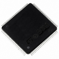
ST10R272LT1 STMicroelectronics, ST10R272LT1 Datasheet - Page 13

ST10R272LT1
Manufacturer Part Number
ST10R272LT1
Description
MCU 16BIT ROMLESS LV 100-TQFP
Manufacturer
STMicroelectronics
Series
ST10r
Datasheet
1.ST10R272LT1TR.pdf
(77 pages)
Specifications of ST10R272LT1
Core Processor
ST10
Core Size
16-Bit
Speed
50MHz
Connectivity
EBI/EMI, SSP, UART/USART
Peripherals
POR, PWM, WDT
Number Of I /o
77
Program Memory Type
ROMless
Ram Size
1K x 8
Voltage - Supply (vcc/vdd)
3 V ~ 3.6 V
Oscillator Type
Internal
Operating Temperature
0°C ~ 70°C
Package / Case
100-TQFP, 100-VQFP
Controller Family/series
ST10
No. Of I/o's
77
Ram Memory Size
1KB
Cpu Speed
50MHz
No. Of Timers
5
Embedded Interface Type
SPI, USART
No. Of Pwm Channels
1
Rohs Compliant
Yes
Processor Series
ST10R2x
Core
ST10
Data Bus Width
16 bit
Data Ram Size
1 KB
Interface Type
SSP, USART
Maximum Clock Frequency
50 MHz
Number Of Programmable I/os
77
Number Of Timers
5
Maximum Operating Temperature
+ 70 C
Mounting Style
SMD/SMT
Minimum Operating Temperature
0 C
On-chip Adc
16 bit
Case
QFP
Lead Free Status / RoHS Status
Lead free / RoHS Compliant
Eeprom Size
-
Program Memory Size
-
Data Converters
-
Lead Free Status / Rohs Status
Details
Available stocks
Company
Part Number
Manufacturer
Quantity
Price
Company:
Part Number:
ST10R272LT1
Manufacturer:
PANASONIC
Quantity:
30 000
Part Number:
ST10R272LT1
Manufacturer:
ST
Quantity:
20 000
Company:
Part Number:
ST10R272LT1/TR
Manufacturer:
STMicroelectronics
Quantity:
10 000
4
The main core of the CPU contains a 4-stage instruction pipeline, a MAC multiply-
accumulation unit, a separate multiply and divide unit, a bit-mask generator and a barrel
shifter. Most instructions can be executed in one machine cycle requiring 40ns at 50MHz CPU
clock.
The CPU includes an actual register context consisting of 16 wordwide GPRs physically
located in the on-chip RAM area. A Context Pointer (CP) register determines the base
address of the active register bank to be accessed by the CPU. The number of register banks
is only restricted by the available internal RAM space. For easy parameter passing, one
register bank may overlap others.
A system stack of up to 1024 bytes is provided as a storage for temporary data. The system
stack is allocated in the on-chip RAM area, and it is accessed by the CPU via the stack pointer
(SP) register. Two separate SFRs, STKOV and STKUN, are compared against the stack
pointer value during each stack access to detect stack overflow or underflow.
CENTRAL PROCESSING UNIT
Data Pg. Ptrs
BUSCON 0
BUSCON 1
BUSCON 2
BUSCON 3
BUSCON 4
SYSCON
Exec. Unit
Instr. Ptr
Instr. Reg
PSW
STKOV
STKUN
4-Stage
Pipeline
SP
Figure 4 CPU block diagram
ADDRSEL 1
ADDRSEL 2
ADDRSEL 3
ADDRSEL 4
Code Seg. Ptr.
Bit-Mask Gen.
Mul./Div.-HW
Context Ptr
Barrel-Shift
CPU
16-Bit
MDH
MDL
ALU
ST10R272L - CENTRAL PROCESSING UNIT
IDX0
QR0
QX0
Registers
Purpose
General
R15
R0
QR1
IDX1
QX1
16
16
1KByte
Internal
RAM
R15
R0
13/77
1


