STM32F102C8T6TR STMicroelectronics, STM32F102C8T6TR Datasheet - Page 17
STM32F102C8T6TR
Manufacturer Part Number
STM32F102C8T6TR
Description
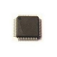
MCU 32BIT ARM 64K FLASH 48-LQFP
Manufacturer
STMicroelectronics
Series
STM32r
Datasheet
1.STEVAL-MKI109V1.pdf
(69 pages)
Specifications of STM32F102C8T6TR
Core Processor
ARM® Cortex-M3™
Core Size
32-Bit
Speed
48MHz
Connectivity
I²C, IrDA, LIN, SPI, UART/USART, USB
Peripherals
DMA, PDR, POR, PVD, PWM, Temp Sensor, WDT
Number Of I /o
37
Program Memory Size
64KB (64K x 8)
Program Memory Type
FLASH
Ram Size
10K x 8
Voltage - Supply (vcc/vdd)
2 V ~ 3.6 V
Data Converters
A/D 10x12b
Oscillator Type
Internal
Operating Temperature
-40°C ~ 85°C
Package / Case
48-LQFP
Processor Series
STM32F102x
Core
ARM Cortex M3
Data Bus Width
32 bit
Data Ram Size
10 KB
Interface Type
I2C, SPI, USART
Maximum Clock Frequency
48 MHz
Number Of Programmable I/os
37
Number Of Timers
6
Operating Supply Voltage
2 V to 3.6 V
Maximum Operating Temperature
+ 85 C
Mounting Style
SMD/SMT
3rd Party Development Tools
EWARM, EWARM-BL, MDK-ARM, RL-ARM, ULINK2
Minimum Operating Temperature
- 40 C
On-chip Adc
12 bit, 10 Channel
For Use With
497-10030 - STARTER KIT FOR STM32497-6438 - BOARD EVALUTION FOR STM32 512K
Lead Free Status / RoHS Status
Lead free / RoHS Compliant
Eeprom Size
-
Lead Free Status / Rohs Status
Details
Available stocks
Company
Part Number
Manufacturer
Quantity
Price
Company:

Part Number:
STM32F102C8T6TR
Manufacturer:
STMicroelectronics
Quantity:
10 000


STM32F102x8, STM32F102xB
Description
Universal synchronous/asynchronous receiver transmitter (USART)
The available USART interfaces communicate at up to 2.25 Mbit/s. They provide hardware
management of the CTS and RTS signals, support IrDA SIR ENDEC, are ISO 7816
compliant and have LIN Master/Slave capability.
The USART interfaces can be served by the DMA controller.
Serial peripheral interface (SPI)
Two SPIs are able to communicate up to 12 Mbit/s in slave and master modes in full-duplex
and simplex communication modes. The 3-bit prescaler gives 8 master mode frequencies
and the frame is configurable to 8 bits or 16 bits. The hardware CRC generation/verification
supports basic SD Card/MMC modes.
Both SPIs can be served by the DMA controller.
Universal serial bus (USB)
The STM32F102xx medium-density USB access line embeds a USB device peripheral
compatible with the USB Full-speed 12 Mbs. The USB interface implements a full-speed (12
Mbit/s) function interface. It has software configurable endpoint setting and suspend/resume
support. The dedicated 48 MHz clock is generated from the internal main PLL (the clock
source must use a HSE crystal oscillator).
GPIOs (general-purpose inputs/outputs)
Each of the GPIO pins can be configured by software as output (push-pull or open-drain), as
input (with or without pull-up or pull-down) or as peripheral alternate function. Most of the
GPIO pins are shared with digital or analog alternate functions. All GPIOs are high current-
capable except for analog inputs.
The I/Os alternate function configuration can be locked if needed following a specific
sequence in order to avoid spurious writing to the I/Os registers.
ADC (analog to digital converter)
The 12-bit analog to digital converter has up to 16 external channels and performs
conversions in single-shot or scan modes. In scan mode, automatic conversion is performed
on a selected group of analog inputs.
The ADC can be served by the DMA controller.
An analog watchdog feature allows very precise monitoring of the converted voltage of one,
some or all selected channels. An interrupt is generated when the converted voltage is
outside the programmed thresholds.
Temperature sensor
The temperature sensor has to generate a a voltage that varies linearly with temperature.
The conversion range is between 2 V < V
< 3.6 V. The temperature sensor is internally
DDA
connected to the ADC_IN16 input channel which is used to convert the sensor output
voltage into a digital value.
Serial wire JTAG debug port (SWJ-DP)
The ARM SWJ-DP Interface is embedded. and is a combined JTAG and serial wire debug
port that enables either a serial wire debug or a JTAG probe to be connected to the target.
The JTAG TMS and TCK pins are shared respectively with SWDIO and SWCLK and a
specific sequence on the TMS pin is used to switch between JTAG-DP and SW-DP.
Doc ID 15056 Rev 3
17/69
Related parts for STM32F102C8T6TR
Image
Part Number
Description
Manufacturer
Datasheet
Request
R

Part Number:
Description:
STMicroelectronics [RIPPLE-CARRY BINARY COUNTER/DIVIDERS]
Manufacturer:
STMicroelectronics
Datasheet:
Part Number:
Description:
STMicroelectronics [LIQUID-CRYSTAL DISPLAY DRIVERS]
Manufacturer:
STMicroelectronics
Datasheet:

Part Number:
Description:
BOARD EVAL FOR MEMS SENSORS
Manufacturer:
STMicroelectronics
Datasheet:
Part Number:
Description:
NPN TRANSISTOR POWER MODULE
Manufacturer:
STMicroelectronics
Datasheet:
Part Number:
Description:
TURBOSWITCH ULTRA-FAST HIGH VOLTAGE DIODE
Manufacturer:
STMicroelectronics
Datasheet:
Part Number:
Description:
Manufacturer:
STMicroelectronics
Datasheet:
Part Number:
Description:
DIODE / SCR MODULE
Manufacturer:
STMicroelectronics
Datasheet:
Part Number:
Description:
DIODE / SCR MODULE
Manufacturer:
STMicroelectronics
Datasheet:
Part Number:
Description:
Search -----> STE16N100
Manufacturer:
STMicroelectronics
Datasheet:
Part Number:
Description:
Search ---> STE53NA50
Manufacturer:
STMicroelectronics
Datasheet:
Part Number:
Description:
NPN Transistor Power Module
Manufacturer:
STMicroelectronics
Datasheet:
Part Number:
Description:
DIODE / SCR MODULE
Manufacturer:
STMicroelectronics
Datasheet: