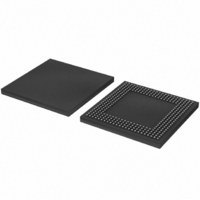
LPC3180FEL320,551 NXP Semiconductors, LPC3180FEL320,551 Datasheet - Page 11

LPC3180FEL320,551
Manufacturer Part Number
LPC3180FEL320,551
Description
IC ARM9 MCU 208MHZ 320-LFBGA
Manufacturer
NXP Semiconductors
Series
LPC3000r
Specifications of LPC3180FEL320,551
Program Memory Type
ROMless
Package / Case
320-LFBGA
Core Processor
ARM9
Core Size
16/32-Bit
Speed
208MHz
Connectivity
EBI/EMI, I²C, MMC, SPI, UART/USART, USB OTG
Peripherals
DMA, PWM, WDT
Number Of I /o
55
Ram Size
64K x 8
Voltage - Supply (vcc/vdd)
1.1 V ~ 3.3 V
Data Converters
A/D 3x10b
Oscillator Type
External
Operating Temperature
-40°C ~ 85°C
Processor Series
LPC31
Core
ARM926EJ-S
Data Bus Width
16 bit, 32 bit
Data Ram Size
64 KB
Interface Type
I2C/SPI/UART/USB
Maximum Clock Frequency
208 MHz
Number Of Programmable I/os
55
Number Of Timers
2
Operating Supply Voltage
3 V
Maximum Operating Temperature
+ 85 C
Mounting Style
SMD/SMT
3rd Party Development Tools
MDK-ARM, RL-ARM, ULINK2, LPC3180-DEV-KIT
Development Tools By Supplier
OM10096
Minimum Operating Temperature
- 40 C
On-chip Adc
3-ch x 10-bit
Package
320LFBGA
Device Core
ARM926EJ-S
Family Name
LPC3100
Maximum Speed
208 MHz
Lead Free Status / RoHS Status
Lead free / RoHS Compliant
For Use With
622-1018 - EVAL KIT FOR LP3180568-4063 - KIT DEV LPC3180568-4062 - DEBUGGER J-LINK JTAG568-4061 - DEBUGGER U-LINK2 JTAG FOR NXP
Eeprom Size
-
Program Memory Size
-
Lead Free Status / Rohs Status
Lead free / RoHS Compliant
Other names
935281874551
LPC3180FEL320-S
LPC3180FEL320-S
LPC3180FEL320-S
LPC3180FEL320-S
Available stocks
Company
Part Number
Manufacturer
Quantity
Price
Company:
Part Number:
LPC3180FEL320,551
Manufacturer:
NXP Semiconductors
Quantity:
10 000
NXP Semiconductors
Table 3.
LPC3180_01_1
Preliminary data sheet
Symbol
U5_TX
U6_IRRX/
PIO_INP[21]
U6_IRTX
U7_HCTS/
PIO_INP[22]
U7_RX/
PIO_INP[23]
U7_TX
USB_ATX_INT_N
USB_DAT_VP/
U5_RX
USB_I2C_SCL
USB_I2C_SDA
USB_OE_TP_N
USB_SE0_VM/
U5_TX
VDD12
VDD_AD28
VDD_CORE12_01 to
VDD_CORE12_03,
VDD_CORE12_05 to
VDD_CORE12_08
VDD_COREFXD12_01,
VDD_COREFXD12_02
VDD_IOA
VDD_IOB
VDD_IOC
VDD_IOD
VDD_OSC12
VDD_PLL397_12
VDD_PLLHCLK_12
VDD_PLLUSB_12
VDD_RTC12
VDD_RTCCORE12
VDD_RTCOSC12
LPC 3180/01 Pin description
Pin
C4
A1
D5
B2
C3
B3
AA7
AA8
AC8
AD7
AD6
AB7
B14
D24, E21
AA2, D6, K21, L3,
AA12, AB6, AB18
C10, D18
B7, B4
AA4
AA19, AA15, AB11,
AC7
U4, G4,
D20
C22
A22
B22
C12
C11
C14
…continued
Rev. 00.08 — 20 November 2008
I
Type Description
O
I/O
I
O
I
I
I
I
O
I
I/O
I
I/O
I/O
I/O
I/O
O
I
I
I
I
I
I
I
I
I
I
I
I
I
I
16/32-bit ARM microcontroller with external memory interface
UART 5 transmit data output
U6_IRRX — UART 6 receive data input; can be IrDA data
PIO_INP[21] — general purpose input to PIO_INP_STATE register
UART 6 transmit data output; can be IrDA data
U7_HCTS — UART 7 hardware flow control (CTS) input
PIO_INP[22] — general purpose input to PIO_INP_STATE register
U7_RX — UART 7 receive data input
PIO_INP[23] — general purpose input to PIO_INP_STATE register
UART 7 transmit data output
USB interrupt from external transceiver
USB_DAT_VP — USB transmit data
U5_RX — UART 5 receive data input
serial clock for USB I
serial data for USB I
USB transmit enable for DAT/SE0
USB_SE0_VM — USB single ended zero transmit
U5_TX — UART 5 transmit data output
1.2 V power supply for various internal functional blocks that are not
included with VDD_CORE or VDD_COREFXD
3.0 V power supply and positive reference voltage for the ADC
1.2 V core main power supply for the CPU and other core logic; this
voltage may be reduced to 0.9 V when the core is running at or
below 13 MHz; the HIGHCORE pin may be used to signal this
condition to an external voltage switch
1.2 V core secondary power supply voltage for the CPU and other
core logic; this supply cannot be reduced in the same manner as the
VDD_CORE12 supply
1.8 V or 3.0 V power supply for I/O pins that may operate from either
a 1.8 V range or a 3 V range
1.8 V or 3.0 V power supply for I/O pins that may operate from either
a 1.8 V range or a 3 V range
1.8 V or 3.0 V power supply for I/O pins that may operate from either
a 1.8 V range or a 3 V range
1.8 V or 3.0 V power supply for I/O pins that may operate from either
a 1.8 V range or a 3 V range
1.2 V power supply for the main oscillator
1.2 V power supply for the 397x PLL
1.2 V power supply for the HCLK PLL
1.2 V power supply for the USB PLL
1.2 V power supply for the RTC block
1.2 V power supply for the RTC block
1.2 V power supply for the 32 kHz RTC oscillator
2
2
C-bus
C-bus
LPC3180/01
© NXP B.V. 2008. All rights reserved.
11 of 56


