LPC2368FET100,518 NXP Semiconductors, LPC2368FET100,518 Datasheet - Page 9
LPC2368FET100,518
Manufacturer Part Number
LPC2368FET100,518
Description
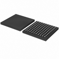
IC ARM7 MCU FLASH 512K 100TFBGA
Manufacturer
NXP Semiconductors
Series
LPC2300r
Datasheet
1.LPC2364FBD100551.pdf
(59 pages)
Specifications of LPC2368FET100,518
Program Memory Type
FLASH
Program Memory Size
512KB (512K x 8)
Package / Case
100-TFBGA
Core Processor
ARM7
Core Size
16/32-Bit
Speed
72MHz
Connectivity
CAN, Ethernet, I²C, Microwire, MMC, SPI, SSI, SSP, UART/USART, USB
Peripherals
Brown-out Detect/Reset, DMA, I²S, POR, PWM, WDT
Number Of I /o
70
Ram Size
58K x 8
Voltage - Supply (vcc/vdd)
3 V ~ 3.6 V
Data Converters
A/D 6x10b; D/A 1x10b
Oscillator Type
Internal
Operating Temperature
-40°C ~ 85°C
Processor Series
LPC23
Core
ARM7TDMI-S
Data Bus Width
16 bit, 32 bit
Data Ram Size
58 KB
Interface Type
CAN/I2C/I2S/SPI/SSP/UART/USB
Maximum Clock Frequency
72 MHz
Number Of Programmable I/os
70
Number Of Timers
4
Operating Supply Voltage
3.3 V
Maximum Operating Temperature
+ 85 C
Mounting Style
SMD/SMT
3rd Party Development Tools
MDK-ARM, RL-ARM, ULINK2, SAB-TFBGA100, MCB2360, MCB2360U, MCB2360UME
Development Tools By Supplier
OM10095, OM11042
Minimum Operating Temperature
- 40 C
On-chip Adc
6-ch x 10-bit
On-chip Dac
1-ch x 10-bit
Package
100TFBGA
Device Core
ARM7TDMI-S
Family Name
LPC2000
Maximum Speed
72 MHz
Lead Free Status / RoHS Status
Lead free / RoHS Compliant
For Use With
568-4917 - DEVELOPMENT BOARD FOR LPC2368622-1022 - BOARD SCKT ADAPTER FOR TFBGA100MCB2360UME - BOARD EVAL MCB2360 + ULINK-MEMCB2360U - BOARD EVAL MCB2360 + ULINK2622-1019 - BOARD FOR LPC2106 48-LQFP568-4014 - BOARD EVAL FOR LPC236X ARM568-3999 - BOARD EVAL FOR LPC23 ARM MCU
Eeprom Size
-
Lead Free Status / Rohs Status
Lead free / RoHS Compliant
Other names
935285102518
LPC2368FET100-T
LPC2368FET100-T
LPC2368FET100-T
LPC2368FET100-T
Available stocks
Company
Part Number
Manufacturer
Quantity
Price
Company:

Part Number:
LPC2368FET100,518
Manufacturer:
NXP Semiconductors
Quantity:
10 000


NXP Semiconductors
Table 4.
LPC2364_65_66_67_68_6
Product data sheet
Symbol
P0[6]/
I2SRX_SDA/
SSEL1/MAT2[0]
P0[7]/
I2STX_CLK/
SCK1/MAT2[1]
P0[8]/
I2STX_WS/
MISO1/MAT2[2]
P0[9]/
I2STX_SDA/
MOSI1/MAT2[3]
P0[10]/TXD2/
SDA2/MAT3[0]
P0[11]/RXD2/
SCL2/MAT3[1]
P0[15]/TXD1/
SCK0/SCK
P0[16]/RXD1/
SSEL0/SSEL
P0[17]/CTS1/
MISO0/MISO
Pin description
Pin
79
78
77
76
48
49
62
63
61
[1]
[1]
[1]
[1]
[1]
[1]
[1]
[1]
[1]
…continued
Ball
B8
A9
C8
A10
H7
K9
F10
F8
F9
[1]
[1]
[1]
[1]
[1]
[1]
[1]
[1]
[1]
Type
I/O
I/O
I/O
O
I/O
I/O
I/O
O
I/O
I/O
I/O
O
I/O
I/O
I/O
O
I/O
O
I/O
O
I/O
I
I/O
O
I/O
O
I/O
I/O
I/O
I
I/O
I/O
I/O
I
I/O
I/O
Description
P0[6] — General purpose digital input/output pin.
I2SRX_SDA — Receive data. It is driven by the transmitter and read by the
receiver. Corresponds to the signal SD in the I
SSEL1 — Slave Select for SSP1.
MAT2[0] — Match output for Timer 2, channel 0.
P0[7] — General purpose digital input/output pin.
I2STX_CLK — Transmit Clock. It is driven by the master and received by
the slave. Corresponds to the signal SCK in the I
SCK1 — Serial Clock for SSP1.
MAT2[1] — Match output for Timer 2, channel 1.
P0[8] — General purpose digital input/output pin.
I2STX_WS — Transmit Word Select. It is driven by the master and
received by the slave. Corresponds to the signal WS in the I
specification.
MISO1 — Master In Slave Out for SSP1.
MAT2[2] — Match output for Timer 2, channel 2.
P0[9] — General purpose digital input/output pin.
I2STX_SDA — Transmit data. It is driven by the transmitter and read by the
receiver. Corresponds to the signal SD in the I
MOSI1 — Master Out Slave In for SSP1.
MAT2[3] — Match output for Timer 2, channel 3.
P0[10] — General purpose digital input/output pin.
TXD2 — Transmitter output for UART2.
SDA2 — I
MAT3[0] — Match output for Timer 3, channel 0.
P0[11] — General purpose digital input/output pin.
RXD2 — Receiver input for UART2.
SCL2 — I
MAT3[1] — Match output for Timer 3, channel 1.
P0[15] — General purpose digital input/output pin.
TXD1 — Transmitter output for UART1.
SCK0 — Serial clock for SSP0.
SCK — Serial clock for SPI.
P0[16] — General purpose digital input/output pin.
RXD1 — Receiver input for UART1.
SSEL0 — Slave Select for SSP0.
SSEL — Slave Select for SPI.
P0[17] — General purpose digital input/output pin.
CTS1 — Clear to Send input for UART1.
MISO0 — Master In Slave Out for SSP0.
MISO — Master In Slave Out for SPI.
Rev. 06 — 1 February 2010
2
2
C2 clock input/output (this is not an open-drain pin).
C2 data input/output (this is not an open-drain pin).
LPC2364/65/66/67/68
Single-chip 16-bit/32-bit microcontrollers
2
2
S-bus specification.
S-bus specification.
2
S-bus specification.
© NXP B.V. 2010. All rights reserved.
2
S-bus
9 of 59
Related parts for LPC2368FET100,518
Image
Part Number
Description
Manufacturer
Datasheet
Request
R

Part Number:
Description:
Single-chip 16-bit/32-bit microcontrollers/ up to 512 kB flash
Manufacturer:
NXP Semiconductors
Datasheet:

Part Number:
Description:
MCU, MPU & DSP Development Tools EVAL BOARD FOR NXP LPC2368 + ULINK2
Manufacturer:
Keil Tools

Part Number:
Description:
MCU, MPU & DSP Development Tools EVAL BOARD FOR NXP LPC2368
Manufacturer:
Keil Tools

Part Number:
Description:
MCU, MPU & DSP Development Tools EVAL BOARD FOR NXP LPC2368 + ULINK-ME
Manufacturer:
Keil Software
Part Number:
Description:
NXP Semiconductors designed the LPC2420/2460 microcontroller around a 16-bit/32-bitARM7TDMI-S CPU core with real-time debug interfaces that include both JTAG andembedded trace
Manufacturer:
NXP Semiconductors
Datasheet:

Part Number:
Description:
NXP Semiconductors designed the LPC2458 microcontroller around a 16-bit/32-bitARM7TDMI-S CPU core with real-time debug interfaces that include both JTAG andembedded trace
Manufacturer:
NXP Semiconductors
Datasheet:
Part Number:
Description:
NXP Semiconductors designed the LPC2468 microcontroller around a 16-bit/32-bitARM7TDMI-S CPU core with real-time debug interfaces that include both JTAG andembedded trace
Manufacturer:
NXP Semiconductors
Datasheet:
Part Number:
Description:
NXP Semiconductors designed the LPC2470 microcontroller, powered by theARM7TDMI-S core, to be a highly integrated microcontroller for a wide range ofapplications that require advanced communications and high quality graphic displays
Manufacturer:
NXP Semiconductors
Datasheet:
Part Number:
Description:
NXP Semiconductors designed the LPC2478 microcontroller, powered by theARM7TDMI-S core, to be a highly integrated microcontroller for a wide range ofapplications that require advanced communications and high quality graphic displays
Manufacturer:
NXP Semiconductors
Datasheet:
Part Number:
Description:
The Philips Semiconductors XA (eXtended Architecture) family of 16-bit single-chip microcontrollers is powerful enough to easily handle the requirements of high performance embedded applications, yet inexpensive enough to compete in the market for hi
Manufacturer:
NXP Semiconductors
Datasheet:
Part Number:
Description:
The XA-S3 device is a member of Philips Semiconductors? XA(eXtended Architecture) family of high performance 16-bitsingle-chip microcontrollers
Manufacturer:
NXP Semiconductors
Datasheet:

Part Number:
Description:
The NXP BlueStreak LH75401/LH75411 family consists of two low-cost 16/32-bit System-on-Chip (SoC) devices
Manufacturer:
NXP Semiconductors
Datasheet:
Part Number:
Description:
The NXP LPC3130/3131 combine an 180 MHz ARM926EJ-S CPU core, high-speed USB2
Manufacturer:
NXP Semiconductors
Datasheet:
Part Number:
Description:
The NXP LPC3141 combine a 270 MHz ARM926EJ-S CPU core, High-speed USB 2
Manufacturer:
NXP Semiconductors