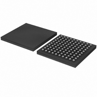
LPC2368FET100,518 NXP Semiconductors, LPC2368FET100,518 Datasheet - Page 12

LPC2368FET100,518
Manufacturer Part Number
LPC2368FET100,518
Description
IC ARM7 MCU FLASH 512K 100TFBGA
Manufacturer
NXP Semiconductors
Series
LPC2300r
Datasheet
1.LPC2364FBD100551.pdf
(59 pages)
Specifications of LPC2368FET100,518
Program Memory Type
FLASH
Program Memory Size
512KB (512K x 8)
Package / Case
100-TFBGA
Core Processor
ARM7
Core Size
16/32-Bit
Speed
72MHz
Connectivity
CAN, Ethernet, I²C, Microwire, MMC, SPI, SSI, SSP, UART/USART, USB
Peripherals
Brown-out Detect/Reset, DMA, I²S, POR, PWM, WDT
Number Of I /o
70
Ram Size
58K x 8
Voltage - Supply (vcc/vdd)
3 V ~ 3.6 V
Data Converters
A/D 6x10b; D/A 1x10b
Oscillator Type
Internal
Operating Temperature
-40°C ~ 85°C
Processor Series
LPC23
Core
ARM7TDMI-S
Data Bus Width
16 bit, 32 bit
Data Ram Size
58 KB
Interface Type
CAN/I2C/I2S/SPI/SSP/UART/USB
Maximum Clock Frequency
72 MHz
Number Of Programmable I/os
70
Number Of Timers
4
Operating Supply Voltage
3.3 V
Maximum Operating Temperature
+ 85 C
Mounting Style
SMD/SMT
3rd Party Development Tools
MDK-ARM, RL-ARM, ULINK2, SAB-TFBGA100, MCB2360, MCB2360U, MCB2360UME
Development Tools By Supplier
OM10095, OM11042
Minimum Operating Temperature
- 40 C
On-chip Adc
6-ch x 10-bit
On-chip Dac
1-ch x 10-bit
Package
100TFBGA
Device Core
ARM7TDMI-S
Family Name
LPC2000
Maximum Speed
72 MHz
Lead Free Status / RoHS Status
Lead free / RoHS Compliant
For Use With
568-4917 - DEVELOPMENT BOARD FOR LPC2368622-1022 - BOARD SCKT ADAPTER FOR TFBGA100MCB2360UME - BOARD EVAL MCB2360 + ULINK-MEMCB2360U - BOARD EVAL MCB2360 + ULINK2622-1019 - BOARD FOR LPC2106 48-LQFP568-4014 - BOARD EVAL FOR LPC236X ARM568-3999 - BOARD EVAL FOR LPC23 ARM MCU
Eeprom Size
-
Lead Free Status / Rohs Status
Lead free / RoHS Compliant
Other names
935285102518
LPC2368FET100-T
LPC2368FET100-T
LPC2368FET100-T
LPC2368FET100-T
Available stocks
Company
Part Number
Manufacturer
Quantity
Price
Company:
Part Number:
LPC2368FET100,518
Manufacturer:
NXP Semiconductors
Quantity:
10 000
NXP Semiconductors
Table 4.
LPC2364_65_66_67_68_6
Product data sheet
Symbol
P1[20]/PWM1[2]/
SCK0
P1[21]/PWM1[3]/
SSEL0
P1[22]/MAT1[0]
P1[23]/PWM1[4]/
MISO0
P1[24]/PWM1[5]/
MOSI0
P1[25]/MAT1[1]
P1[26]/PWM1[6]/
CAP0[0]
P1[27]/CAP0[1]
P1[28]/
PCAP1[0]/
MAT0[0]
P1[29]/
PCAP1[1]/
MAT0[1]
P1[30]/V
AD0[4]
P1[31]/SCK1/
AD0[5]
P2[0] to P2[31]
P2[0]/PWM1[1]/
TXD1/
TRACECLK
BUS
Pin description
/
Pin
34
35
36
37
38
39
40
43
44
45
21
20
75
[1]
[1]
[1]
[1]
[1]
[1]
[1]
[1]
[1]
[1]
[2]
[2]
[1]
…continued
Ball
K4
F5
J5
K5
H5
G5
K6
K7
J7
G6
H1
F4
B9
[1]
[1]
[1]
[2]
[1]
[1]
[1]
[1]
[1]
[1]
[2]
[1]
[1]
Type
I/O
O
I/O
I/O
O
I/O
I/O
O
I/O
O
I/O
I/O
O
I/O
I/O
O
I/O
O
I
I/O
I
I/O
I
O
I/O
I
O
I/O
I
I
I/O
I/O
I
I/O
I/O
O
O
O
Description
P1[20] — General purpose digital input/output pin.
PWM1[2] — Pulse Width Modulator 1, channel 2 output.
SCK0 — Serial clock for SSP0.
P1[21] — General purpose digital input/output pin.
PWM1[3] — Pulse Width Modulator 1, channel 3 output.
SSEL0 — Slave Select for SSP0.
P1[22] — General purpose digital input/output pin.
MAT1[0] — Match output for Timer 1, channel 0.
P1[23] — General purpose digital input/output pin.
PWM1[4] — Pulse Width Modulator 1, channel 4 output.
MISO0 — Master In Slave Out for SSP0.
P1[24] — General purpose digital input/output pin.
PWM1[5] — Pulse Width Modulator 1, channel 5 output.
MOSI0 — Master Out Slave in for SSP0.
P1[25] — General purpose digital input/output pin.
MAT1[1] — Match output for Timer 1, channel 1.
P1[26] — General purpose digital input/output pin.
PWM1[6] — Pulse Width Modulator 1, channel 6 output.
CAP0[0] — Capture input for Timer 0, channel 0.
P1[27] — General purpose digital input/output pin.
CAP0[1] — Capture input for Timer 0, channel 1.
P1[28] — General purpose digital input/output pin.
PCAP1[0] — Capture input for PWM1, channel 0.
MAT0[0] — Match output for Timer 0, channel 0.
P1[29] — General purpose digital input/output pin.
PCAP1[1] — Capture input for PWM1, channel 1.
MAT0[1] — Match output for Timer 0, channel 0.
P1[30] — General purpose digital input/output pin.
V
Note: This signal must be HIGH for USB reset to occur.
AD0[4] — A/D converter 0, input 4.
P1[31] — General purpose digital input/output pin.
SCK1 — Serial Clock for SSP1.
AD0[5] — A/D converter 0, input 5.
Port 2: Port 2 is a 32-bit I/O port with individual direction controls for each
bit. The operation of Port 2 pins depends upon the pin function selected via
the pin connect block. Pins 14 through 31 of this port are not available.
P2[0] — General purpose digital input/output pin.
PWM1[1] — Pulse Width Modulator 1, channel 1 output.
TXD1 — Transmitter output for UART1.
TRACECLK — Trace Clock.
Rev. 06 — 1 February 2010
BUS
— Monitors the presence of USB bus power. (LPC2364/66/68 only)
LPC2364/65/66/67/68
Single-chip 16-bit/32-bit microcontrollers
© NXP B.V. 2010. All rights reserved.
12 of 59


